- 您現(xiàn)在的位置:買賣IC網 > PDF目錄383961 > TMX320DM648ZUT900 (Texas Instruments, Inc.) Digital Media Processor PDF資料下載
參數(shù)資料
| 型號: | TMX320DM648ZUT900 |
| 廠商: | Texas Instruments, Inc. |
| 英文描述: | Digital Media Processor |
| 中文描述: | 數(shù)字媒體處理器 |
| 文件頁數(shù): | 42/166頁 |
| 文件大小: | 1341K |
| 代理商: | TMX320DM648ZUT900 |
第1頁第2頁第3頁第4頁第5頁第6頁第7頁第8頁第9頁第10頁第11頁第12頁第13頁第14頁第15頁第16頁第17頁第18頁第19頁第20頁第21頁第22頁第23頁第24頁第25頁第26頁第27頁第28頁第29頁第30頁第31頁第32頁第33頁第34頁第35頁第36頁第37頁第38頁第39頁第40頁第41頁當前第42頁第43頁第44頁第45頁第46頁第47頁第48頁第49頁第50頁第51頁第52頁第53頁第54頁第55頁第56頁第57頁第58頁第59頁第60頁第61頁第62頁第63頁第64頁第65頁第66頁第67頁第68頁第69頁第70頁第71頁第72頁第73頁第74頁第75頁第76頁第77頁第78頁第79頁第80頁第81頁第82頁第83頁第84頁第85頁第86頁第87頁第88頁第89頁第90頁第91頁第92頁第93頁第94頁第95頁第96頁第97頁第98頁第99頁第100頁第101頁第102頁第103頁第104頁第105頁第106頁第107頁第108頁第109頁第110頁第111頁第112頁第113頁第114頁第115頁第116頁第117頁第118頁第119頁第120頁第121頁第122頁第123頁第124頁第125頁第126頁第127頁第128頁第129頁第130頁第131頁第132頁第133頁第134頁第135頁第136頁第137頁第138頁第139頁第140頁第141頁第142頁第143頁第144頁第145頁第146頁第147頁第148頁第149頁第150頁第151頁第152頁第153頁第154頁第155頁第156頁第157頁第158頁第159頁第160頁第161頁第162頁第163頁第164頁第165頁第166頁
www.ti.com
P
3.2.6
PINMUX Register
TMS320DM647/TMS320DM648
Digital Media Processor
SPRS372–MAY 2007
Writes to these registers are locked/blocked by default. To enable writes to these registers, write
0xADDDECAF to the KEY_REG. After enabling writes to protected registers by doing the above, the
register writes should occur within 10000 CPU/6 cycles, after which the key will be reset.
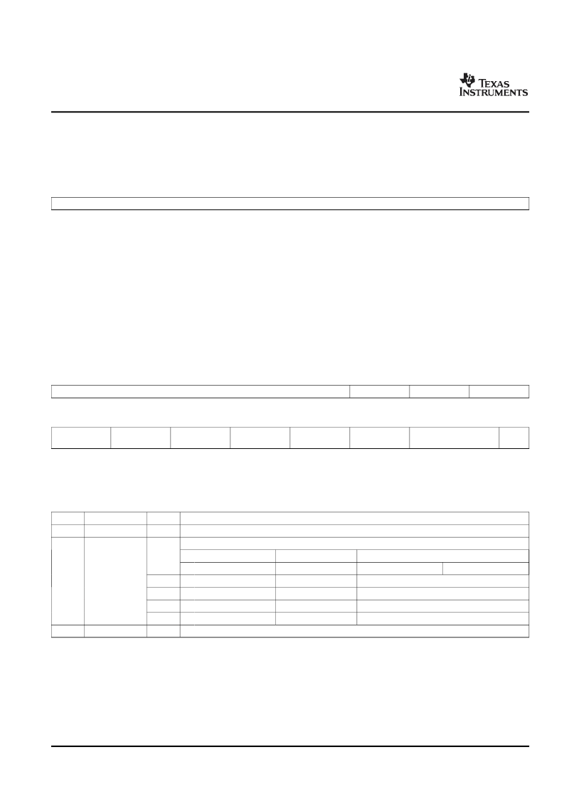
Figure 3-5. KEY_REG
31
0
KEY_REG
W-0x00000000
LEGEND: R/W = Read/Write; R = Read only; -
n
= value after reset
All pin multiplexing options are controlled by software via PINMUX register (except the ones mentioned in
Table 3-7
, whose default is selected by configuration pins). This PINMUX register reside within the system
module portion of the CFG bus memory map. The format of the registers and a description of the pins
they control are in the following sections.
The PINMux Register controls all the software-controlled pin muxing. The register format is shown in
Figure 3-6
. A brief description of each field is shown in
Table 3-6
.
Figure 3-6. PINMUX Register
31
22
21
GPIO_EN
20
19
Reserved
18
17
16
Reserved
VPI_EN
R-0000 0000 00
R/W-00
R-00
R/W-00
15
VP34_EN
14
13
12
11
Reserved
10
9
8
7
Reserved
6
5
4
3
1
0
SPI_UART_EN
MCASP_EN
VLYNQ_EN
Reserved
TIMER
_EN
R/W-00
R/W-00
R-00
R/W-00
R-00
R/W-00
R-000
R/W-0
LEGEND: R/W = Read/Write; R = Read only; -
n
= value after reset
Table 3-6. PINMUX Register Field Descriptions
Bit
31:22
21:20
Field
Reserved
GPIO_EN
Value
Description
Reserved
Controls the pin muxing between Video Port 0 and the GPIO[12:15]
UNMUXED
(1)
UNMUXED
(2)
.VP0D16-19
VP0D02-09/CLK/CTL
3-state
3-state
Enable
3-state
Reserved
SECONDARY MUXED
(3)
VP0D12-15
3-state
3-state
VP0D12-15
GP12-15
GP12-15
00
01
10
11
3-state
3-state
Enable
Enable
19:18
Reserved
(1)
(2)
(3)
The complete list of pins: U20, U21, U22, R18.
The complete list of pins: Y23, V23, Y22, V22, U23, W20, V18, U18, V19, W21, T18, U19, V20.
The complete list of pins: V21, T19, T20, T21.
Device Configuration
42
Submit Documentation Feedback
相關PDF資料 |
PDF描述 |
|---|---|
| TMS320LC31PQL | DIGITAL SIGNAL PROCESSORS |
| TMX320C6414TGLZ | FIXED-POINT DIGITAL SIGNAL PROCESSORS |
| TMX320C6415TGLZ | FIXED-POINT DIGITAL SIGNAL PROCESSORS |
| TMXF28155 | 155/51 Mbits/s SONET/SDH(155/51 M位/秒 SONET/SDH) |
| TN28F001BX-T150 | 1-MBIT (128K x 8) BOOT BLOCK FLASH MEMORY |
相關代理商/技術參數(shù) |
參數(shù)描述 |
|---|---|
| TMX320DM648ZUTQ7 | 制造商:Texas Instruments 功能描述: |
| TMX320DM8147BCYE0 | 制造商:Texas Instruments 功能描述: |
| TMX320DM8147BCYE2 | 制造商:Texas Instruments 功能描述: |
| TMX320DM8148BCYE | 功能描述:數(shù)字信號處理器和控制器 - DSP, DSC DaVinci Dig Media Proc RoHS:否 制造商:Microchip Technology 核心:dsPIC 數(shù)據(jù)總線寬度:16 bit 程序存儲器大小:16 KB 數(shù)據(jù) RAM 大小:2 KB 最大時鐘頻率:40 MHz 可編程輸入/輸出端數(shù)量:35 定時器數(shù)量:3 設備每秒兆指令數(shù):50 MIPs 工作電源電壓:3.3 V 最大工作溫度:+ 85 C 封裝 / 箱體:TQFP-44 安裝風格:SMD/SMT |
| TMX320DM8148CCYE2 | 制造商:Texas Instruments 功能描述: |
發(fā)布緊急采購,3分鐘左右您將得到回復。