- 您現(xiàn)在的位置:買賣IC網(wǎng) > PDF目錄384004 > TLC320AD80C (Texas Instruments, Inc.) Audio Processor Subsystem PDF資料下載
參數(shù)資料
| 型號: | TLC320AD80C |
| 廠商: | Texas Instruments, Inc. |
| 英文描述: | Audio Processor Subsystem |
| 中文描述: | 音頻處理器子系統(tǒng) |
| 文件頁數(shù): | 21/36頁 |
| 文件大小: | 219K |
| 代理商: | TLC320AD80C |
第1頁第2頁第3頁第4頁第5頁第6頁第7頁第8頁第9頁第10頁第11頁第12頁第13頁第14頁第15頁第16頁第17頁第18頁第19頁第20頁當(dāng)前第21頁第22頁第23頁第24頁第25頁第26頁第27頁第28頁第29頁第30頁第31頁第32頁第33頁第34頁第35頁第36頁
2–10
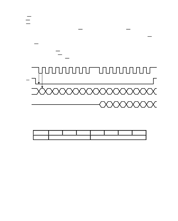
The CS input must make a low to high transition in order to specify a new control register address. When
the CS input is set to 1, the serial command data output (CDOUT) is placed in a high-impedance state. When
the CS input is cleared to 0, the CDOUT output is held low during nonvalid data intervals.
The serial control port is activated when the CS signal (active low) goes low. The CS line must be low prior
to data transactions and must remain low for the duration of the transaction. The serial command data input
(CDIN) is sampled on the rising edge of SCLK. The CDIN data is MSB first and unsigned. While the CS input
is low, the SCLK input must idle high when there is no valid data to be transferred. The first byte of CDIN
data after CS activation is set up as a serial control command. The serial control command includes a 4-bit
control register address [D(3–0)] and a control port direction bit (D7). The second byte of data is set up as
control register data. The CS input must make a low-to-high transition in order to specify a new control
register address. When the CS input goes high, the serial command data output (CDOUT) is placed in a
high-impedance state. When the CS input goes low, the CDOUT output is held low during nonvalid data
intervals.
D7
D6
D5
D4
D3
D2
D1
D0
D7
D6
D5
D4
D3
D2
D1
D0
D7
D6
D5
D4
D3
D2
D1
D0
MSB
LSB
Serial Control Command
MSB
LSB
Serial Data
SCLK
CS
CDIN
CDOUT
Figure 2–5. Serial Interface Timing
2.5.2
The serial control command format is shown below.
Serial Control Command Format
ááááááááááááááááááááá
The serial control command fields are defined as:
ááááááááá
ááááááááááááááááááááá
WR – Serial interface direction
When this bit is 1:
The serial interface is in write mode.
Serial data is sent control register specified in the serial control command
When this bit is 0:
The serial interface is in read mode.
The control register data is output to CDOUT according to the control register address.
ADDR(3–0) – Control register address specifies the TLC320AD80 register being accessed.
相關(guān)PDF資料 |
PDF描述 |
|---|---|
| TLC320AD81CDBT | Stereo Audio Digital Equalizer DC |
| TLC320AD81C | Stereo Audio Digital Equalizer DC |
| TLC339CDB | LinCMOSE MICROPOWER QUAD COMPARATORS |
| TLC339CDBR | LinCMOSE MICROPOWER QUAD COMPARATORS |
| TLC34058-110M | 256 ?24 COLOR PALETTE |
相關(guān)代理商/技術(shù)參數(shù) |
參數(shù)描述 |
|---|---|
| TLC320AD80CPM | 制造商:Rochester Electronics LLC 功能描述:- Bulk 制造商:Texas Instruments 功能描述: |
| TLC320AD81C | 制造商:TI 制造商全稱:Texas Instruments 功能描述:Stereo Audio Digital Equalizer DC |
| TLC320AD81CDBT | 制造商:Rochester Electronics LLC 功能描述:- Tape and Reel |
| TLC320AD90 | 制造商:TI 制造商全稱:Texas Instruments 功能描述:Stereo Audio Codec |
| TLC320AD91 | 制造商:TI 制造商全稱:Texas Instruments 功能描述:Stereo Audio Codec |
發(fā)布緊急采購,3分鐘左右您將得到回復(fù)。