- 您現(xiàn)在的位置:買賣IC網(wǎng) > PDF目錄1969 > SSTUB32S869BHLFT (IDT, Integrated Device Technology Inc)IC REGIST BUFF 14BIT DDR2 150BGA PDF資料下載
參數(shù)資料
| 型號(hào): | SSTUB32S869BHLFT |
| 廠商: | IDT, Integrated Device Technology Inc |
| 文件頁(yè)數(shù): | 12/17頁(yè) |
| 文件大小: | 0K |
| 描述: | IC REGIST BUFF 14BIT DDR2 150BGA |
| 產(chǎn)品變化通告: | Product Discontinuation 09/Dec/2011 |
| 標(biāo)準(zhǔn)包裝: | 2,000 |
| 類型: | 緩沖器 |
| Tx/Rx類型: | LVCMOS |
| 延遲時(shí)間: | 3.0ns |
| 電容 - 輸入: | 3.5pF |
| 電源電壓: | 1.7 V ~ 1.9 V |
| 安裝類型: | 表面貼裝 |
| 封裝/外殼: | 150-TFBGA |
| 供應(yīng)商設(shè)備封裝: | 150-CABGA(8x13) |
| 包裝: | 帶卷 (TR) |
第1頁(yè)第2頁(yè)第3頁(yè)第4頁(yè)第5頁(yè)第6頁(yè)第7頁(yè)第8頁(yè)第9頁(yè)第10頁(yè)第11頁(yè)當(dāng)前第12頁(yè)第13頁(yè)第14頁(yè)第15頁(yè)第16頁(yè)第17頁(yè)
4
ICSSSTUB32S869B
Advance Information
1203—04/11/06
The ICSSSTUB32S869B is 14-bit 1:2 registered buffer with parity is designed for 1.7 V to 1.9 V VDD operation.
All clock and data inputs are compatible with the JEDEC standard for SSTL_18. The control inputs are LVCMOS. All
outputs are 1.8 V CMOS drivers optimized to drive the DDR2 DIMM load. They provide 50% more dynamic driver
strength than the standard SSTU32864 outputs.
The ICSSSTUB32S869B operates from a differential clock (CK and CK). Data are registered at the crossing of CK going
high, and CK going low.
The device supports low-power standby operation. When the reset input (RESET) is low, the differential input receivers
are disabled, and undriven (floating) data, clock and reference voltage (VREF) inputs are allowed. In addition, when
RESET is low all registers are reset, and all outputs except PTYERR1# are forced low. The LVCMOS RESET input must
always be held at a valid logic high or low level.
To ensure defined outputs from the register before a stable clock has been supplied, RESET must be held in the low
state during power up.
In the DDR2 RDIMM application, RESET is specified to be completely asynchronous with respect to CK and CK.
Therefore, no timing relationship can be guaranteed between the two. When entering reset, the register will be cleared
and the outputs will be driven low quickly, relative to the time to disable the differential input receivers. However, when
coming out of reset, the register will become active quickly, relative to the time to enable the differential input receivers.
ICSSSTUB32S869B must ensure that the outputs remain low as long as the data inputs are low, the clock is stable
during the time from the low-to-high transition of RESET and the input receivers are fully enabled. This will ensures that
there are no glitches on the output.
The device monitors both DCS and CSR inputs and will gate the Qn, PPO1 (Paritial-Parity-Out) and PTYERR1# (Parity
Error) Parity outputs from changing states when both DCS and CSR are high. If either DCS or CSR input is low, the
Qn, PPO1 and PTYERR1# outputs will function normally. The RESET input has priority over the DCS and CSR controls
and will force the Qn and PPO outputs low and the PTYERR1# high.
The ICSSSTUB32S869B includes a parity checking function. The ICSSSTUB32S869B accepts a parity bit from the
memory controller at its input pin PARIN1 one or two cycles after the corresponding data input, compares it with the
data received on the D-inputs and indicates on its opendrain PTYERR1 pin (active low) whether a parity error has
occurred. The number of cycles depends on the setting of C1, see Figure 6 and 7.
When used as a single device, the C1 input is tied low. When used in pairs, the C1 inputs is tied low for the first register
(front) and the C1 input is tied high for the second register. When used as a single register, the PPO1 and PTYERR1#
signals are produced two clock cycles after the corresponding data input. When used in pairs, the PTYERR1# signals
of the first register are left floating. The PPO1 outputs of the first register are cascaded to the PARIN1 signals on the
second register (back). The PPO1 and PTYERR1# signals of the second register are produced three clock cycles after
the corresponding data input. Parity implimentation and device wiring for single and dual die is described in Figure 1.
If an error occurs, and the PTYERR1# is driven low, it stays low for two clock cycles or until RESET is driven low. The
DIMM-dependent signals (DCKE, DCS, CSR and DODT) are not included in the parity check computations.
All registers used on an individual DIMM must be of the same configuration, i.e single or dual die.
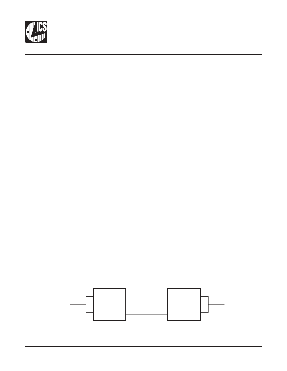
General Description
PTYERR1# W1
Register 1
(Front)
Parin1, W4
NC, A8
Parin
PPO1, W8
Parin1, W4
NC, A4
Register 2
(Back)
NC, A8
NC, A11
Set C1 = 0 for Register 1; Set C1 = 1 for Register 2. NC denotes No Connect.
..
Figure 1 — Parity implementation and device wiring for SSTU32S869 and SSTU32D869
相關(guān)PDF資料 |
PDF描述 |
|---|---|
| ST16C1450CJ28-F | IC UART FIFO 1B 28PLCC |
| ST16C2450CJ44-F | IC DUART 44PLCC |
| ST16C2550CJ44-F | IC DUART FIFO 16B 44PLCC |
| ST16C2552IJ44TR-F | IC UART FIFO 16B DUAL 44PLCC |
| ST16C450CJ44-F | IC UART SINGLE 44PLCC |
相關(guān)代理商/技術(shù)參數(shù) |
參數(shù)描述 |
|---|---|
| SSTUBF32866AHLF | 制造商:Integrated Device Technology Inc 功能描述:REGISTERED BFFR SGL 25-CH CMOS 96CABGA - Trays |
| SSTUBF32866AHLFT | 制造商:Integrated Device Technology Inc 功能描述:REGISTERED BFFR SGL 25-CH CMOS 96LFBGA - Tape and Reel |
| SSTUBF32866BHLF | 制造商:Integrated Device Technology Inc 功能描述:DDR 800 REGISTER. BGA 96 - Bulk |
| SSTUBF32866BHLF8 | 制造商:Integrated Device Technology Inc 功能描述:DDR 800 REGISTER. BGA 96 - Tape and Reel |
| SSTUBV32866BHLFT/M | 制造商:Integrated Device Technology Inc 功能描述:SSTUBV32866BHLFT/M - Tape and Reel |
發(fā)布緊急采購(gòu),3分鐘左右您將得到回復(fù)。