- 您現(xiàn)在的位置:買賣IC網(wǎng) > PDF目錄98081 > SK12430PJT 800 MHz, OTHER CLOCK GENERATOR, PQCC28 PDF資料下載
參數(shù)資料
| 型號(hào): | SK12430PJT |
| 元件分類: | 時(shí)鐘產(chǎn)生/分配 |
| 英文描述: | 800 MHz, OTHER CLOCK GENERATOR, PQCC28 |
| 封裝: | PLASTIC, LCC-28 |
| 文件頁(yè)數(shù): | 16/16頁(yè) |
| 文件大?。?/td> | 225K |
| 代理商: | SK12430PJT |
第1頁(yè)第2頁(yè)第3頁(yè)第4頁(yè)第5頁(yè)第6頁(yè)第7頁(yè)第8頁(yè)第9頁(yè)第10頁(yè)第11頁(yè)第12頁(yè)第13頁(yè)第14頁(yè)第15頁(yè)當(dāng)前第16頁(yè)

9
Revision 1/.ebruary 8, 2001
www.semtech.com
HIGH-PER.ORMANCE PRODUCTS
SK12430
ADVANCED
25
20
15
10
5
0
400
500
600
700
800
N = 2
N = 4
N = 8
RMS
Jitter
(ps)
Output Frequency (MHz)
Application Information (continued)
Generally the resistor/capacitor filter will be cheaper,
easier to implement and provide an adequate level
of supply filtering.
The SK12430 provides sub-nanosecond output edge
rates and thus a good power supply bypassing
scheme is a must.
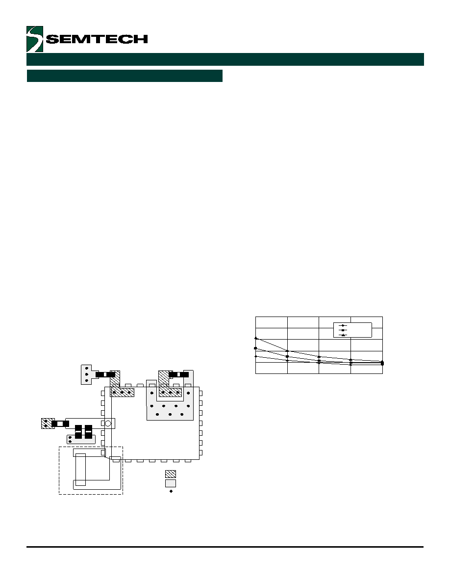
Figure 6 shows
a representa-
tive board layout for the SK12430.
There exists
many different potential board layouts and the one
pictured below is but one. The important aspect of
the layout in Figure 6 is the low impedance connec-
tions between VCC and GND for the bypass capaci-
tors.
Combining good quality general purpose chip
capacitors with good PCB layout techniques will pro-
duce effective capacitor resonances at frquencies
adequate to supply the instantaneous switching cur-
rent for the 1240 outputs. It is imperative that low
inductance chip capacitors are used; it is equally
important that the board layout does not introduce
back all of the inductance saved by using the leadless
capacitors.
Thin interconnect traces between the
capacitor and the power plane should beavoided and
multiple large vias should be used to tie the capaci-
tors to the buried power planes.
Fat interconnect
and large vias will help to minimize layout induced
inductance and thus maximize the series resonant
point of the bypass capacitors.
the crystal is relatively small.
It is imperative that no
actively switching signals cross under the crystal as
crosstalk energy coupled to these lines could significantly
impact the jitter of the device. Special attention should
be paid to the layout of the crystal to ensure a stable,
jitter free interface between the crystal and the on-board
oscillator.
Although the SK12430 has several design features to
minimize the susceptibility to power supply noise (iso-
lated power and grounds and fully differential PLL), there
still may be applications in which overall performance is
being degraded due to system power supply noise. The
power supply filter and bypass schemes discussed in
this section should be adequate to eliminate power sup-
ply noise related problems in most designs.
Jitter Performance of the SK12430
The SK12430 exhibits long term and cycle-to-cycle jitter
which rivals that of SAW based oscillators.
This jitter
performance comes with the added flexibility one gets
with a synthesizer of a fixed frequency oscillator.
1
= VCC
= GND
= Via
R1
C3
C1
C2
Xtal
R1 = 10 15W
C1 = 0.01 F
C2 = 22 F
C3 = 0.1 F
Figure 6. PCB Board Layout for the SK12430
Note: The dotted lines circling the crystal oscillator
connection to the device. The oscillator is a series
resonant circuit and the voltage amplitude across
Figure 7. RMS Jitter versus VCO Frequency
Figure 7 illustrates the RMS jitter performance of the
SK12430 across its specified VCO frequency range. Note
that the jitter is a function of both the output frequency
as well as the VCO frequency
However, the VCO fre-
quency shows a much stronger dependence. The data
presented has not been compensated for trigger jitter
and this fact provides a measure of guardband to the
reported data.
The typical method of measuring the
jitter is to accumulate a large number of cycles, create a
histogram of the edge placements and record peak-to-
peak as well as standard deviations of the jitter. Care
must be taken that the measured edge is the edge im-
mediately following the trigger edge.
相關(guān)PDF資料 |
PDF描述 |
|---|---|
| SK12439PJ | 800 MHz, OTHER CLOCK GENERATOR, PQCC28 |
| SK12439PJT | 800 MHz, OTHER CLOCK GENERATOR, PQCC28 |
| SL15100ZIT-XXX | 200 MHz, OTHER CLOCK GENERATOR, PDSO8 |
| SL15100ZCT-XXX | 200 MHz, OTHER CLOCK GENERATOR, PDSO8 |
| SL15102DI-XXX | OTHER CLOCK GENERATOR, DSO8 |
相關(guān)代理商/技術(shù)參數(shù) |
參數(shù)描述 |
|---|---|
| SK125 | 制造商:Thomas & Betts 功能描述: |
| SK1250C | 制造商:DEC 制造商全稱:DEC 功能描述:12 AMP SCHOTTKY BARRIER RECTIFIERS |
| SK12516 | 制造商:Cooper Wiring Devices 功能描述: |
| SK1260C | 制造商:DEC 制造商全稱:DEC 功能描述:12 AMP SCHOTTKY BARRIER RECTIFIERS |
| SK1270C | 制造商:DEC 制造商全稱:DEC 功能描述:12 AMP SCHOTTKY BARRIER RECTIFIERS |
發(fā)布緊急采購(gòu),3分鐘左右您將得到回復(fù)。