- 您現(xiàn)在的位置:買賣IC網(wǎng) > PDF目錄98080 > SI5327D-C-GMR (SILICON LABORATORIES) 243 MHz, PROC SPECIFIC CLOCK GENERATOR, QCC36 PDF資料下載
參數(shù)資料
| 型號: | SI5327D-C-GMR |
| 廠商: | SILICON LABORATORIES |
| 元件分類: | 時鐘產(chǎn)生/分配 |
| 英文描述: | 243 MHz, PROC SPECIFIC CLOCK GENERATOR, QCC36 |
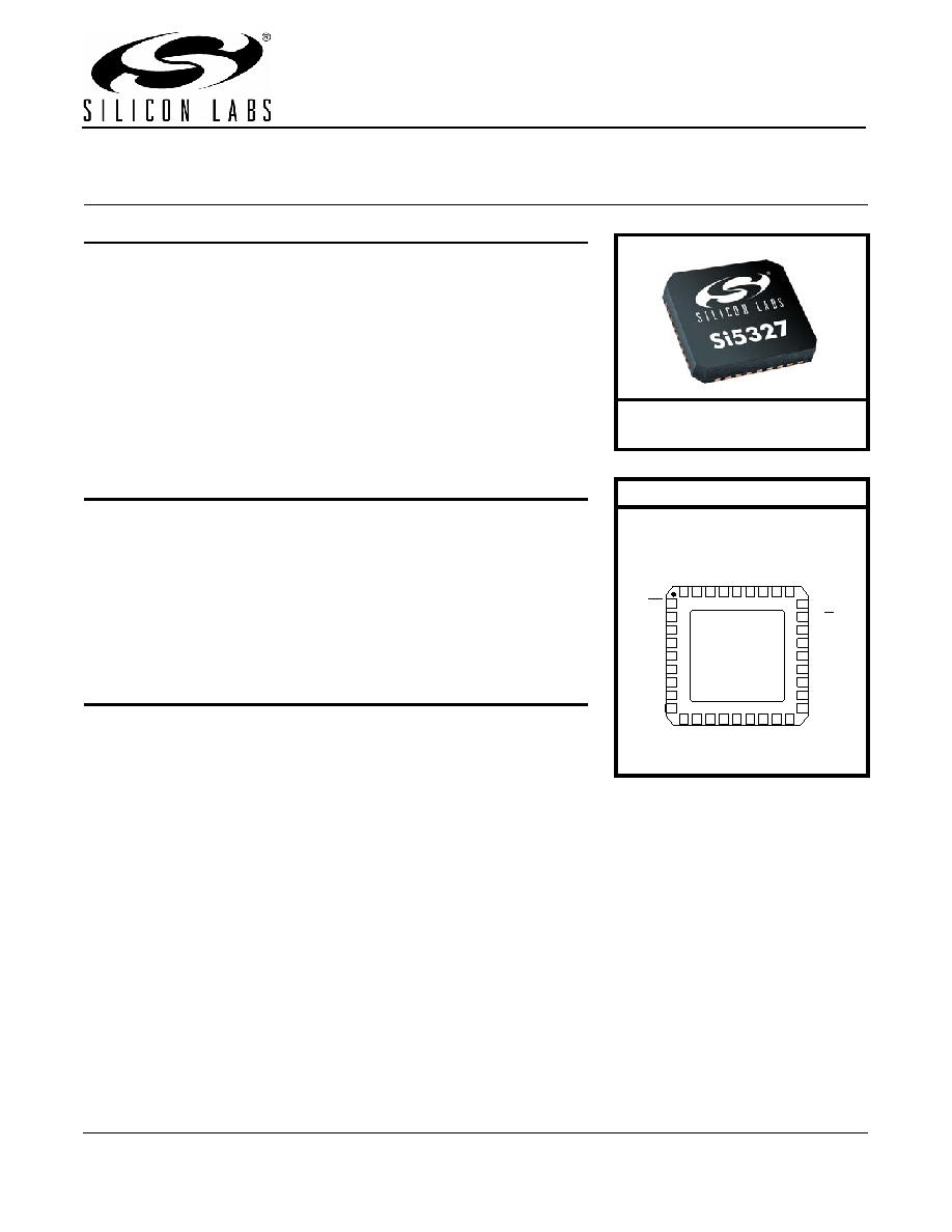
| 封裝: | 6 X 6 MM, ROHS COMPLIANT, MO-220VJJD, QFN-36 |
| 文件頁數(shù): | 1/60頁 |
| 文件大?。?/td> | 715K |
| 代理商: | SI5327D-C-GMR |
當前第1頁第2頁第3頁第4頁第5頁第6頁第7頁第8頁第9頁第10頁第11頁第12頁第13頁第14頁第15頁第16頁第17頁第18頁第19頁第20頁第21頁第22頁第23頁第24頁第25頁第26頁第27頁第28頁第29頁第30頁第31頁第32頁第33頁第34頁第35頁第36頁第37頁第38頁第39頁第40頁第41頁第42頁第43頁第44頁第45頁第46頁第47頁第48頁第49頁第50頁第51頁第52頁第53頁第54頁第55頁第56頁第57頁第58頁第59頁第60頁

Preliminary Rev. 0.4 5/11
Copyright 2011 by Silicon Laboratories
Si5327
This information applies to a product under development. Its characteristics and specifications are subject to change without notice.
Si5327
A NY F REQUENCY P RECISION C LOCK M ULTIPLIER/J ITTER
A TTENUATOR
Features
Applications
Description
The Si5327 is a jitter-attenuating precision clock multiplier for applications
requiring sub 1 ps jitter performance. The Si5327 accepts two input clocks ranging
from 2 kHz to 710 MHz and generates two output clocks ranging from 2 kHz to
808 MHz. The two outputs are divided down separately from a common source.
The Si5327 can also use its crystal oscillator as a clock source for frequency
synthesis. The device provides virtually any frequency translation combination
across this operating range. The Si5327 input clock frequency and clock
multiplication ratio are programmable through an I2C or SPI interface. The Si5327
is based on Silicon Laboratories' 3rd-generation DSPLL technology, which
provides frequency synthesis and jitter attenuation in a highly integrated PLL
solution that eliminates the need for external VCXO and loop filter components.
The DSPLL loop bandwidth is digitally programmable, providing jitter performance
optimization at the application level. Operating from a single 1.8, 2.5, or 3.3 V
supply, the Si5327 is ideal for providing clock multiplication and jitter attenuation in
high performance timing applications.
Generates any frequency from 2 kHz
to 808 MHz from an input frequency
of 2kHz to 710MHz
Ultra-low jitter clock outputs with jitter
generation as low as 0.5 ps rms
(12 kHz–20 MHz)
Integrated loop filter with selectable
loop bandwidth (4 to 525 Hz)
Meets OC-192 GR-253-CORE jitter
specifications
Dual clock inputs with manually
controlled hitless switching
Free run and holdover modes
Support for ITU G.709 and custom
FEC ratios (255/238, 255/237,
255/236)
LOL and LOS alarm outputs
Digitally-controlled output phase
adjustment
I2C or SPI programmable
Single 1.8, 2.5, 3.3 V supply
Small size: 6 x 6 mm 36-lead QFN
Pb-free, ROHS compliant
Dual clock outputs with
programmable signal format
(LVPECL, LVDS, CML, CMOS)
SONET/SDH OC-48/OC-192/STM-
16/STM-64 line cards
ITU G.709 and custom FEC line
cards
GbE/10GbE, 1/2/4/8/10G Fibre
Channel line cards
Synchronous Ethernet
Optical modules
Wireless repeaters/
wireless backhaul
Data converter clocking
xDSL
PDH clock synthesis
Test and measurement
Broadcast video
Ordering Information:
See page 54.
Pin Assignments
1
2
3
29
30
31
32
33
34
35
36
20
21
22
23
24
25
26
27
10 11 12 13 14 15 16 17
4
5
6
7
8
NC
RST
LOS2
INT_LOS1
GND
VDD
XA
VD
D
RA
TE
CK
IN
2+
CK
IN
2–
NC
GN
D
CKI
N1+
CK
IN
1–
CKSEL
SCL
SDA_SDO
A1
A2_SS
SDI
CK
OU
T1
–
NC
GN
D
VD
D
NC
CK
OUT
2–
CK
OUT
2+
CM
OD
E
GND
Pad
A0
NC
9
18
19
28
XB
LOL
NC
CK
OU
T1
+
相關(guān)PDF資料 |
PDF描述 |
|---|---|
| SI5334B-A00122-GM | PLL BASED CLOCK DRIVER, QCC24 |
| SI5334C-A00129-GMR | PLL BASED CLOCK DRIVER, QCC24 |
| SI5334C-A00153-GM | PLL BASED CLOCK DRIVER, QCC24 |
| SI5334C-A00160-GM | PLL BASED CLOCK DRIVER, QCC24 |
| SI5334A-A00102-GM | PLL BASED CLOCK DRIVER, QCC24 |
相關(guān)代理商/技術(shù)參數(shù) |
參數(shù)描述 |
|---|---|
| Si5327-EVB | 功能描述:時鐘和定時器開發(fā)工具 SI5327 EVAL BOARD RoHS:否 制造商:Texas Instruments 產(chǎn)品:Evaluation Modules 類型:Clock Conditioners 工具用于評估:LMK04100B 頻率:122.8 MHz 工作電源電壓:3.3 V |
| SI5328 | 制造商:SILABS 制造商全稱:SILABS 功能描述:ITU-T G.8262 SYNCHRONOUS ETHERNET JITTER-ATTENUATING CLOCK MULTIPLIER |
| SI5328B-C-GM | 制造商:Silicon Laboratories Inc 功能描述:G.8262 SYNCE CLOCK MULTIPLIER/JITTER ATTENUATOR - Trays 制造商:Silicon Laboratories Inc 功能描述:IC CLK MULTIPLIER ETH 36QFN |
| SI5328B-C-GMR | 制造商:Silicon Laboratories Inc 功能描述:IC CLK MULTIPLIER ETH 36QFN |
| SI5328C-C-GM | 制造商:Silicon Laboratories Inc 功能描述:G.8262 SYNCE CLOCK MULTIPLIER/JITTER ATTENUATOR - Trays 制造商:Silicon Laboratories Inc 功能描述:IC TIMING CLOCK 36QFN 制造商:Silicon Laboratories Inc 功能描述:Clock Generators & Support Products G.8262 SyncE Clock Multiplier |
發(fā)布緊急采購,3分鐘左右您將得到回復(fù)。