- 您現(xiàn)在的位置:買賣IC網(wǎng) > PDF目錄98068 > S1C63466F 4-BIT, MROM, 4.1 MHz, MICROCONTROLLER, PQFP144 PDF資料下載
參數(shù)資料
| 型號: | S1C63466F |
| 元件分類: | 微控制器/微處理器 |
| 英文描述: | 4-BIT, MROM, 4.1 MHz, MICROCONTROLLER, PQFP144 |
| 封裝: | PLASTIC, QFP8-144 |
| 文件頁數(shù): | 26/135頁 |
| 文件大小: | 1053K |
| 代理商: | S1C63466F |
第1頁第2頁第3頁第4頁第5頁第6頁第7頁第8頁第9頁第10頁第11頁第12頁第13頁第14頁第15頁第16頁第17頁第18頁第19頁第20頁第21頁第22頁第23頁第24頁第25頁當(dāng)前第26頁第27頁第28頁第29頁第30頁第31頁第32頁第33頁第34頁第35頁第36頁第37頁第38頁第39頁第40頁第41頁第42頁第43頁第44頁第45頁第46頁第47頁第48頁第49頁第50頁第51頁第52頁第53頁第54頁第55頁第56頁第57頁第58頁第59頁第60頁第61頁第62頁第63頁第64頁第65頁第66頁第67頁第68頁第69頁第70頁第71頁第72頁第73頁第74頁第75頁第76頁第77頁第78頁第79頁第80頁第81頁第82頁第83頁第84頁第85頁第86頁第87頁第88頁第89頁第90頁第91頁第92頁第93頁第94頁第95頁第96頁第97頁第98頁第99頁第100頁第101頁第102頁第103頁第104頁第105頁第106頁第107頁第108頁第109頁第110頁第111頁第112頁第113頁第114頁第115頁第116頁第117頁第118頁第119頁第120頁第121頁第122頁第123頁第124頁第125頁第126頁第127頁第128頁第129頁第130頁第131頁第132頁第133頁第134頁第135頁
S1C63466 TECHNICAL MANUAL
EPSON
113
CHAPTER 7: ELECTRICAL CHARACTERISTICS
7.5 Oscillation Characteristics
The oscillation characteristics change depending on the conditions (components used, board pattern,
etc.). Use the following characteristics as reference values.
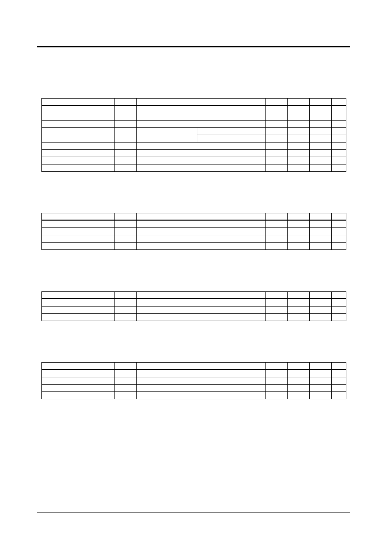
OSC1 crystal oscillation circuit
Item
Oscillation start voltage
Oscillation stop voltage
Built-in capacitance (drain)
Frequency/voltage deviation
Frequency/IC deviation
Frequency adjustment range
Harmonic oscillation start voltage
Permitted leak resistance
Symbol
Vsta
Vstp
CD
f/V
f/IC
f/CG
Vhho
Rleak
Unit
V
pF
ppm
V
M
Max.
5
10
Typ.
14
20
Min.
1.8
-10
10
6.4
200
Condition
tsta
≤3sec (VDD)
tstp
≤10sec (VDD)
Including the parasitic capacitance inside the IC (in chip)
VDD=2.2 to 6.4V
with VDC switching
without VDC switching
CG=5 to 25pF
CG=5pF (VDD)
Between OSC1 and VSS
Unless otherwise specified:
VDD=3.0V, VSS=0V, fOSC1=32.768kHz, CG=25pF, CD=built-in, Ta=-20 to 70
°C
OSC1 CR oscillation circuit
Item
Oscillation frequency dispersion
Oscillation start voltage
Oscillation start time
Oscillation stop voltage
Symbol
fOSC1
Vsta
tsta
Vstp
Unit
%
V
mS
V
Max.
30
3
Typ.
60kHz
Min.
-30
2.2
Condition
(VDD)
VDD=2.2 to 6.4V
(VDD)
Unless otherwise specified:
VDD=3.0V, VSS=0V, RCR1=600k
, Ta=-20 to 70°C
OSC3 ceramic oscillation circuit
Item
Oscillation start voltage
Oscillation start time
Oscillation stop voltage
Symbol
Vsta
tsta
Vstp
Unit
V
mS
V
Max.
5
Typ.
Min.
2.2
Condition
(VDD)
VDD=2.2 to 6.4V
(VDD)
Unless otherwise specified:
VDD=3.0V, VSS=0V, Ceramic oscillator: 4MHz, CGC=CDC=30pF, Ta=-20 to 70
°C
OSC3 CR oscillation circuit
Item
Oscillation frequency dispersion
Oscillation start voltage
Oscillation start time
Oscillation stop voltage
Symbol
fOSC3
Vsta
tsta
Vstp
Unit
%
V
mS
V
Max.
25
3
Typ.
1,800kHz
Min.
-25
2.2
Condition
(VDD)
VDD=2.2 to 6.4V
(VDD)
Unless otherwise specified:
VDD=3.0V, VSS=0V, RCR2=47k
, Ta=-20 to 70°C
相關(guān)PDF資料 |
PDF描述 |
|---|---|
| S1C63567F0A0100 | MICROCONTROLLER, PQFP144 |
| S1C63653F | 4-BIT, FLASH, 4 MHz, MICROCONTROLLER, CQFP100 |
| S1C6F567D0A0100 | MICROCONTROLLER, UUC141 |
| S1C6N3B0D0A0100 | MICROCONTROLLER, UUC54 |
| S1C6P366D0A0100 | 4-BIT, FLASH, 4.1 MHz, MICROCONTROLLER, UUC102 |
相關(guān)代理商/技術(shù)參數(shù) |
參數(shù)描述 |
|---|---|
| S1C63557D04Q000 | 制造商:Seiko Instruments Inc (SII) 功能描述:EPSON MCU 4BIT |
| S1C63567 | 制造商:EPSON 制造商全稱:EPSON 功能描述:4-bit Single Chip Microcomputer |
| S1C63616 | 制造商:EPSON 制造商全稱:EPSON 功能描述:4-bit Single Chip Microcomputer |
| S1C63632 | 制造商:EPSON 制造商全稱:EPSON 功能描述:4-bit Single Chip Microcomputer |
| S1C63653 | 制造商:EPSON 制造商全稱:EPSON 功能描述:CMOS 4-bit Single Chip Microcontroller |
發(fā)布緊急采購,3分鐘左右您將得到回復(fù)。