- 您現(xiàn)在的位置:買賣IC網(wǎng) > PDF目錄384799 > OV6630 (Electronic Theatre Controls, Inc.) SINGLE-CHIP CMOS CIF COLOR DIGITAL CAMERA PDF資料下載
參數(shù)資料
| 型號: | OV6630 |
| 廠商: | Electronic Theatre Controls, Inc. |
| 英文描述: | SINGLE-CHIP CMOS CIF COLOR DIGITAL CAMERA |
| 中文描述: | 單芯片CMOS到岸價格彩色數(shù)碼攝像機(jī) |
| 文件頁數(shù): | 20/29頁 |
| 文件大?。?/td> | 206K |
| 代理商: | OV6630 |
第1頁第2頁第3頁第4頁第5頁第6頁第7頁第8頁第9頁第10頁第11頁第12頁第13頁第14頁第15頁第16頁第17頁第18頁第19頁當(dāng)前第20頁第21頁第22頁第23頁第24頁第25頁第26頁第27頁第28頁第29頁
S INGLE IC CMOS COLOR AND B/W DIGIT AL CAMERAS
during read cycle, the master returns acknowledge except the read
data is the last byte. The master does not perform acknowledge if the
read data is the last byte, indicates that the slave can terminate the
read cycle. Note that the restart feature is not supported here.
Within each byte, MSB is always transferred first. Read/write control
bit is the LSB of the first byte.
Standard I
2
C communications require only two pins: SCL and SDA.
SDA is configured as open drain for bi-directional purpose. A HIGH
to LOW transition on the SDA while SCL is HIGH indicates a
START condition. A LOW to HIGH transition on the SDA while
March 4, 2000
Version 1.0
20
SCL is HIGH indicates a STOP condition. Only a master can generate
START/STOP conditions.
Except for these two special conditions, the protocol that SDA remain
stable during the HIGH period of the clock, SCL. Each bit is allowed
to change state only when SCL is LOW (See Figure * and Figure 10
below).
The OV6630/OV6130 I
2
C supports multi-byte write and multi-byte
read. The master must supply the sub-address. in the write cycle, but
not in the read cycle.
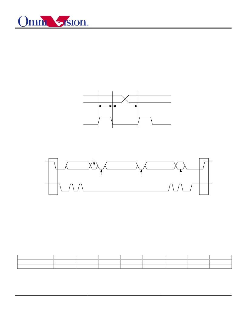
DATA
STABLE
DATA CHANGE
ALLOWED
SDA
SCL
Figure 9. Bit Transfer on the I
2
C Bus
SLAVD ID
SUB ADD
DATA
S
P
A
A
A
RW
SDA
SCL
Figure 10. Data Transfer on the I
2
C Bus
Therefore, OV6630/OV6130 takes the read sub-address from the
previous write cycle. In multi-byte write or multi-byte read cycles, the
sub-address is automatically increment after the first data byte so that
continuous locations can be accessed in one bus cycle. A multi-byte
cycle overwrites its original sub-address; therefore, if a read cycle
immediately follows a multi-byte cycle, you must insert a single byte
write cycle that provides a new sub-address.
OV6630/OV6130 can be power up pin programmed to one-of-eight
slave ID addresses through function pins CS[2:0] (pins 35, 37, 34,
respectively).
Table 15. Slave ID Addresses
CS[2:0]
WRITE ID (hex)
READ ID (hex)
000
C0
C1
001
C4
C5
010
C8
C9
011
CC
CD
100
D0
D1
101
D4
D5
110
D8
D9
111
DC
DD
OV6630/OV6130 supports both single chip and multiple chip
configurations. By asserting MULT (pin 47) to high, the sensor can be
programmed for up to 8 slave ID addresses. Asserting MULT low
configures OV6630/OV6130 for single ID slave address with address
C0 for writes and address C1 for reads. MULT is internally defaulted
to a low condition.
相關(guān)PDF資料 |
PDF描述 |
|---|---|
| OV7410 | SINGLE-CHIP CMOS COLOR PAL CAMERA |
| OV7410P | SINGLE-CHIP CMOS COLOR PAL CAMERA |
| OV7411 | SINGLE-CHIP CMOS COLOR PAL CAMERA |
| OV7411P | SINGLE-CHIP CMOS COLOR PAL CAMERA |
| OV7910 | SINGLE-CHIP CMOS COLOR PAL CAMERA |
相關(guān)代理商/技術(shù)參數(shù) |
參數(shù)描述 |
|---|---|
| OV6680 | 制造商:OMNIVISION 制造商全稱:OMNIVISION 功能描述:optimal low-light sensitivity and pixel performance for video conferencing cameras in 3G mobile phones |
| OV7121 | 制造商:Omnivision Technologies Inc 功能描述: |
| OV7141 | 制造商:未知廠家 制造商全稱:未知廠家 功能描述:OV7640 Color CMOS VGA (640 x 480) CAMERACHIP OV7141 B&W CMOS VGA (640 x 480) CAMERACHIP |
| OV7410 | 制造商:未知廠家 制造商全稱:未知廠家 功能描述:SINGLE-CHIP CMOS COLOR PAL CAMERA |
| OV7410P | 制造商:未知廠家 制造商全稱:未知廠家 功能描述:SINGLE-CHIP CMOS COLOR PAL CAMERA |
發(fā)布緊急采購,3分鐘左右您將得到回復(fù)。