- 您現(xiàn)在的位置:買賣IC網(wǎng) > PDF目錄299551 > NAND512R4A2CZD6E (NUMONYX) 32M X 16 FLASH 1.8V PROM, 15000 ns, PBGA55 PDF資料下載
參數(shù)資料
| 型號(hào): | NAND512R4A2CZD6E |
| 廠商: | NUMONYX |
| 元件分類: | PROM |
| 英文描述: | 32M X 16 FLASH 1.8V PROM, 15000 ns, PBGA55 |
| 封裝: | 8 X 10 MM, 1 MM HEIGHT, ROHS COMPLIANT, VFBGA-55 |
| 文件頁數(shù): | 15/55頁 |
| 文件大?。?/td> | 1377K |
| 代理商: | NAND512R4A2CZD6E |
第1頁第2頁第3頁第4頁第5頁第6頁第7頁第8頁第9頁第10頁第11頁第12頁第13頁第14頁當(dāng)前第15頁第16頁第17頁第18頁第19頁第20頁第21頁第22頁第23頁第24頁第25頁第26頁第27頁第28頁第29頁第30頁第31頁第32頁第33頁第34頁第35頁第36頁第37頁第38頁第39頁第40頁第41頁第42頁第43頁第44頁第45頁第46頁第47頁第48頁第49頁第50頁第51頁第52頁第53頁第54頁第55頁
Device operations
NAND512-A2C
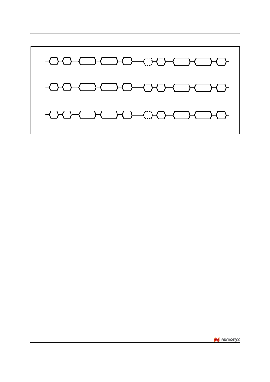
Figure 8.
Pointer operations for programming
6.2
Read memory array
Each operation to read the memory area starts with a pointer operation as shown in the
Section 6.1: Pointer operations. Once the area (main or spare) has been selected using the
Read A, Read B or Read C commands four bus cycles (for 512-Mbit and 1-Gbit devices) or
three bus cycles (for 128-Mbit and 256-Mbit devices) are required to input the address (refer
The device defaults to read A mode after power-up or a reset operation.
When reading the spare area addresses:
●
A0 to A3 (x8 devices)
●
A0 to A2 (x16 devices)
are used to set the start address of the spare area while addresses:
●
A4 to A7 (x8 devices)
●
A3 to A7 (x16 devices)
are ignored.
Once the Read A or Read C commands have been issued they do not need to be reissued
for subsequent read operations as the pointer remains in the respective area. However, the
Read B command is effective for only one operation, once an operation has been executed
in area B the pointer returns automatically to area A and so another Read B command is
required to start another read operation in area B.
Once a Read command is issued two types of operations are available: random read and
page read.
6.2.1
Random read
Each time the command is issued the first read is random read.
ai07591
I/O
Address
Inputs
Data Input
10h
80h
Areas A, B, C can be programmed depending on how much data is input. Subsequent 00h commands can be omitted.
AREA A
00h
Address
Inputs
Data Input
10h
80h
00h
I/O
Address
Inputs
Data Input
10h
80h
Areas B, C can be programmed depending on how much data is input. The 01h command must be re-issued before each program.
AREA B
01h
Address
Inputs
Data Input
10h
80h
01h
I/O
Address
Inputs
Data Input
10h
80h
Only Areas C can be programmed. Subsequent 50h commands can be omitted.
AREA C
50h
Address
Inputs
Data Input
10h
80h
50h
相關(guān)PDF資料 |
PDF描述 |
|---|---|
| NB2762ASNR2G | HF - EMI REDUCER; Package: TSOP-6; No of Pins: 6; Container: Tape and Reel; Qty per Container: 2500 |
| NB2762ASNR2 | EMI REDUCER SERIES; Package: TSOP-6; No of Pins: 6; Container: Tape and Reel; Qty per Container: 2500 |
| NC7SB121P5X | 1-CHANNEL, SGL POLE SGL THROW SWITCH, PDSO5 |
| NCC2222AUB | 800 mA, 50 V, NPN, Si, SMALL SIGNAL TRANSISTOR |
| NCP1216D65R2 | PWM Current-Mode Controller for High-Power Universal Off-line Supplies; Package: SOIC-8 Narrow Body; No of Pins: 8; Container: Tape and Reel; Qty per Container: 2500 |
相關(guān)代理商/技術(shù)參數(shù) |
參數(shù)描述 |
|---|---|
| NAND512R4A2DDI6 | 制造商:Micron Technology Inc 功能描述:NAND - Gel-pak, waffle pack, wafer, diced wafer on film |
| NAND512W3A0AN6 | 功能描述:閃存 NAND & S.MEDIA FLASH RoHS:否 制造商:ON Semiconductor 數(shù)據(jù)總線寬度:1 bit 存儲(chǔ)類型:Flash 存儲(chǔ)容量:2 MB 結(jié)構(gòu):256 K x 8 定時(shí)類型: 接口類型:SPI 訪問時(shí)間: 電源電壓-最大:3.6 V 電源電壓-最小:2.3 V 最大工作電流:15 mA 工作溫度:- 40 C to + 85 C 安裝風(fēng)格:SMD/SMT 封裝 / 箱體: 封裝:Reel |
| NAND512W3A0AN6E | 功能描述:閃存 2.7-3.6V 512M(64Mx8) RoHS:否 制造商:ON Semiconductor 數(shù)據(jù)總線寬度:1 bit 存儲(chǔ)類型:Flash 存儲(chǔ)容量:2 MB 結(jié)構(gòu):256 K x 8 定時(shí)類型: 接口類型:SPI 訪問時(shí)間: 電源電壓-最大:3.6 V 電源電壓-最小:2.3 V 最大工作電流:15 mA 工作溫度:- 40 C to + 85 C 安裝風(fēng)格:SMD/SMT 封裝 / 箱體: 封裝:Reel |
| NAND512W3A0AN6F | 制造商:Micron Technology Inc 功能描述:FLASH PARALLEL 3V/3.3V 512MBIT 64MX8 12US 48TSOP - Tape and Reel |
| NAND512W3A0AV6E | 功能描述:IC FLASH 512MBIT 48WSOP RoHS:是 類別:集成電路 (IC) >> 存儲(chǔ)器 系列:- 標(biāo)準(zhǔn)包裝:576 系列:- 格式 - 存儲(chǔ)器:閃存 存儲(chǔ)器類型:閃存 - NAND 存儲(chǔ)容量:512M(64M x 8) 速度:- 接口:并聯(lián) 電源電壓:2.7 V ~ 3.6 V 工作溫度:-40°C ~ 85°C 封裝/外殼:48-TFSOP(0.724",18.40mm 寬) 供應(yīng)商設(shè)備封裝:48-TSOP 包裝:托盤 其它名稱:497-5040 |
發(fā)布緊急采購,3分鐘左右您將得到回復(fù)。