- 您現(xiàn)在的位置:買賣IC網(wǎng) > PDF目錄384756 > MT48H16M16LFFG (Micron Technology, Inc.) MOBILE SDRAM PDF資料下載
參數(shù)資料
| 型號: | MT48H16M16LFFG |
| 廠商: | Micron Technology, Inc. |
| 英文描述: | MOBILE SDRAM |
| 中文描述: | 移動SDRAM |
| 文件頁數(shù): | 14/58頁 |
| 文件大?。?/td> | 1451K |
| 代理商: | MT48H16M16LFFG |
第1頁第2頁第3頁第4頁第5頁第6頁第7頁第8頁第9頁第10頁第11頁第12頁第13頁當前第14頁第15頁第16頁第17頁第18頁第19頁第20頁第21頁第22頁第23頁第24頁第25頁第26頁第27頁第28頁第29頁第30頁第31頁第32頁第33頁第34頁第35頁第36頁第37頁第38頁第39頁第40頁第41頁第42頁第43頁第44頁第45頁第46頁第47頁第48頁第49頁第50頁第51頁第52頁第53頁第54頁第55頁第56頁第57頁第58頁
14
256Mb: x16 Mobile SDRAM
MobileRamY26L_A.p65 – Pub. 5/02
Micron Technology, Inc., reserves the right to change products or specifications without notice.
2002, Micron Technology, Inc.
256Mb: x16
MOBILE SDRAM
ADVANCE
CLK
T2
T1
T3
T0
t
COMMAND
NOP
ACTIVE
READ or
WRITE
T4
NOP
RCD
DON’T CARE
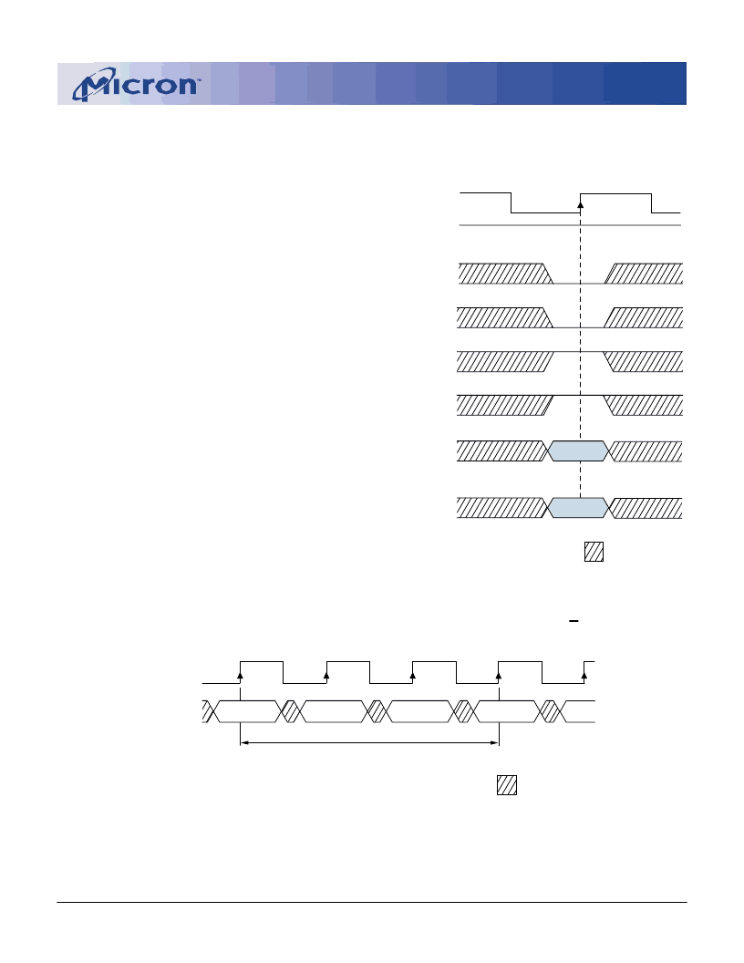
Operation
BANK/ROW ACTIVATION
Before any READ or WRITE commands can be is-
sued to a bank within the SDRAM, a row in that bank
must be “opened.” This is accomplished via the AC-
TIVE command, which selects both the bank and the
row to be activated (see Figure 3).
After opening a row (issuing an ACTIVE command),
a READ or WRITE command may be issued to that row,
subject to the
t
RCD specification.
t
RCD (MIN) should
be divided by the clock period and rounded up to the
next whole number to determine the earliest clock edge
after the ACTIVE command on which a READ or WRITE
command can be entered. For example, a
t
RCD specifi-
cation of 20ns with a 125 MHz clock (8ns period) results
in 2.5 clocks, rounded to 3. This is reflected in Figure 4,
which covers any case where 2 <
t
RCD (MIN)/
t
CK
≤
3.
(The same procedure is used to convert other specifi-
cation limits from time units to clock cycles.)
A subsequent ACTIVE command to a different row
in the same bank can only be issued after the previous
active row has been “closed” (precharged). The mini-
mum time interval between successive ACTIVE com-
mands to the same bank is defined by
t
RC.
A subsequent ACTIVE command to another bank
can be issued while the first bank is being accessed,
which results in a reduction of total row-access over-
head. The minimum time interval between successive
ACTIVE commands to different banks is defined by
t
RRD.
Figure 4
Example: Meeting
t
RCD (MIN) When 2 <
t
RCD (MIN)/
t
CK
<
3
Figure 3
Activating a Specific Row in a
Specific Bank
CS#
WE#
CAS#
RAS#
CKE
CLK
A0-A12
ROW
ADDRESS
DON’T CARE
HIGH
BA0, BA1
BANK
ADDRESS
相關(guān)PDF資料 |
PDF描述 |
|---|---|
| MT49H16M18C | 288Mb SIO REDUCED LATENCY(RLDRAM II) |
| MT49H16M18CFM-xx | 288Mb SIO REDUCED LATENCY(RLDRAM II) |
| MT49H32M9C | 288Mb SIO REDUCED LATENCY(RLDRAM II) |
| MT49H32M9CFM-xx | 288Mb SIO REDUCED LATENCY(RLDRAM II) |
| MT4C1004J | 4 Meg x 1 FPM DRAM(4 M x 1快速頁面模式動態(tài)RAM) |
相關(guān)代理商/技術(shù)參數(shù) |
參數(shù)描述 |
|---|---|
| MT48H16M16LFP-8 LXT | 制造商:Micron Technology Inc 功能描述:16MX16 SSDRAM PLASTIC EXT TEMP PBF TSOP 1.8V - Trays |
| MT48H16M16LFTG-10 IT | 制造商:Micron Technology Inc 功能描述:DRAM Chip Mobile SDRAM 256M-Bit 16Mx16 1.8V 54-Pin TSOP Tray |
| MT48H16M32L2B5-10 | 功能描述:IC SDRAM 512MBIT 100MHZ 90VFBGA RoHS:是 類別:集成電路 (IC) >> 存儲器 系列:- 標準包裝:1 系列:- 格式 - 存儲器:RAM 存儲器類型:SDRAM 存儲容量:256M(8Mx32) 速度:143MHz 接口:并聯(lián) 電源電壓:3 V ~ 3.6 V 工作溫度:-40°C ~ 85°C 封裝/外殼:90-VFBGA 供應(yīng)商設(shè)備封裝:90-VFBGA(8x13) 包裝:托盤 其它名稱:Q2841869 |
| MT48H16M32L2B5-10 IT | 功能描述:IC SDRAM 512MBIT 100MHZ 90VFBGA RoHS:是 類別:集成電路 (IC) >> 存儲器 系列:- 標準包裝:1 系列:- 格式 - 存儲器:RAM 存儲器類型:SDRAM 存儲容量:256M(8Mx32) 速度:143MHz 接口:并聯(lián) 電源電壓:3 V ~ 3.6 V 工作溫度:-40°C ~ 85°C 封裝/外殼:90-VFBGA 供應(yīng)商設(shè)備封裝:90-VFBGA(8x13) 包裝:托盤 其它名稱:Q2841869 |
| MT48H16M32L2B5-10 IT TR | 功能描述:IC SDRAM 512MBIT 100MHZ 90VFBGA RoHS:是 類別:集成電路 (IC) >> 存儲器 系列:- 標準包裝:378 系列:- 格式 - 存儲器:閃存 存儲器類型:FLASH 存儲容量:8M(1M x 8,512K x 16) 速度:110ns 接口:并聯(lián) 電源電壓:2.7 V ~ 3.6 V 工作溫度:-40°C ~ 85°C 封裝/外殼:48-CBGA 供應(yīng)商設(shè)備封裝:48-CBGA(7x7) 包裝:托盤 |
發(fā)布緊急采購,3分鐘左右您將得到回復(fù)。