- 您現(xiàn)在的位置:買賣IC網(wǎng) > PDF目錄371135 > MPC973 (Motorola, Inc.) LOW VOLTAGE PLL CLOCK DRIVER PDF資料下載
參數(shù)資料
| 型號: | MPC973 |
| 廠商: | Motorola, Inc. |
| 英文描述: | LOW VOLTAGE PLL CLOCK DRIVER |
| 中文描述: | 低壓PLL時鐘驅(qū)動器 |
| 文件頁數(shù): | 7/14頁 |
| 文件大小: | 182K |
| 代理商: | MPC973 |
MPC972 MPC973
TIMING SOLUTIONS
BR1333 — Rev 6
7
MOTOROLA
MPC972/973’s to generate two banks of clocks with one
bank divided by 2 and delayed by 180
°
relative to the first.
Using the MPC973 as a Zero Delay Buffer
The external feedback of the MPC973 clock driver allows
for its use as a zero delay buffer. By using one of the outputs
as a feedback to the PLL the propagation delay through the
device is eliminated. The PLL works to align the output edge
with the input reference edge thus producing a near zero
delay. The reference frequency affects the static phase offset
of the PLL and thus the relative delay between the inputs and
outputs. Because the static phase offset is a function of the
reference clock the Tpd of the MPC973 is a function of the
configuration used.
When used as a zero delay buffer the MPC973 will likely
be in a nested clock tree application. For these applications
the MPC973 offers a LVPECL clock input as a PLL reference.
This allows the user to use LVPECL as the primary clock
distribution device to take advantage of its far superior skew
performance. The MPC973 then can lock onto the LVPECL
reference and translate with near zero delay to low skew
LVCMOS outputs. Clock trees implemented in this fashion
will show significantly tighter skews than trees developed
from CMOS fanout buffers.
To calculate the overall uncertainty between the input
reference clock and the output clocks the following approach
should be used. Figure 4 through Figure 7 contain the
performance information required to calculate the overall
uncertainty. Since the overall skew performance is a function
of the input reference frequency all of the graphs provide
relavent data with respect to the input reference frequency.
The overall uncertainty can be broken down into three
parts; the static phase offset variation (Tpd), the I/O phase
jitter and the output skew. If we assume that we have a
75MHz reference clock, from the graphs we can pull the
following information for static phase offset (SPO) and I/O
jitter: the SPO variation will be 300ps (–100ps to +200ps
assuming a TCLK is used) and the I/O jitter will be
±
105ps
(assuming a VCO/6 configuration and a
±
3 sigma for min and
max). The nominal delay from Figure 5 is 50ps so that the
propagation delay between the reference clock and the
feedback clock is 50ps
±
255ps.
Figure 4 can now be used to establish the uncertainty
between the reference clock and all of the outputs for the
MPC973. Figure 4 provides the skew of the MC973 outputs
with respect to the feedback output. From Figure 4, if all of
the outputs are used the propagation delay of the device will
range from –555ps (50ps – 255ps – 350ps) to +705ps (50ps
+ 255ps + 400ps) for a total uncertainty of 1.26ns. This
1.26ns uncertainty would hold true if multiple 973’s are used
in parallel in the application given that the skew between the
reference clock for the devices were zero. Notice from the
data in Figure 4 that if a subset of the outputs were used
significant reductions in uncertainty could be obtained.
SYNC Output Description
In situations where output frequency relationships are not
integer multiples of each other there is a need for a signal for
system synchronization purposes. The SYNC output of the
MPC972/973 is designed to specifically address this need.
The MPC972/973 monitors the relationship between the Qa
and the Qc banks of outputs. It provides a low going pulse,
one period in duration, one period prior to the coincident
rising edges of the Qa and Qc outputs. The duration and the
placement of the pulse is dependent on the higher of the Qa
and Qc output frequencies. The timing diagrams in the data
sheet show the various waveforms for the SYNC output.
Note that the SYNC output is defined for all possible
combinations of the Qa and Qc outputs even though under
some relationships the lower frequency clock could be used
as a synchronizing signal.
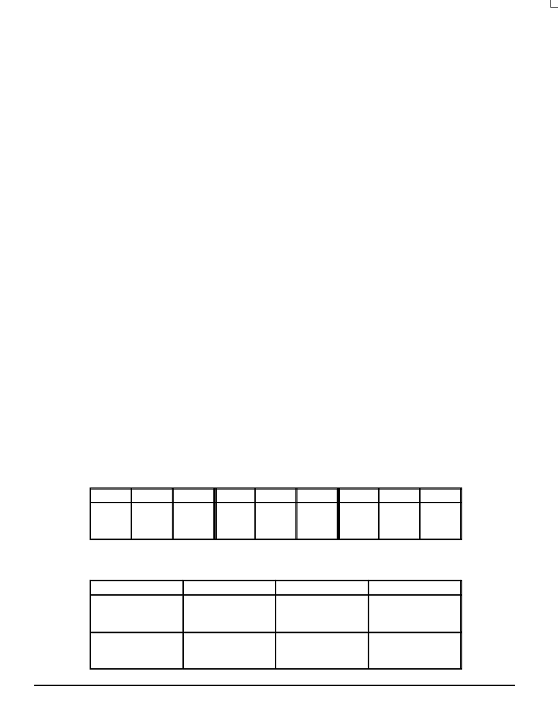
Table 1. Programmable Output Frequency Relationships
(VCO_Sel=‘1’)
fsela1
fsela0
Qa
fselb1
fselb0
Qb
fselc1
fselc0
Qc
0
0
1
1
0
1
0
1
VCO/4
VCO/6
VCO/8
VCO/12
0
0
1
1
0
1
0
1
VCO/4
VCO/6
VCO/8
VCO/10
0
0
1
1
0
1
0
1
VCO/2
VCO/4
VCO/6
VCO/8
Table 2. Programmable Output Frequency Relationships
(VCO_Sel=‘1’)
fselFB2
fselFB1
fselFB0
QFB
0
0
0
0
0
0
1
1
0
1
0
1
VCO/4
VCO/6
VCO/8
VCO/10
1
1
1
1
0
0
1
1
0
1
0
1
VCO/8
VCO/12
VCO/16
VCO/20
相關(guān)PDF資料 |
PDF描述 |
|---|---|
| MPC974 | 3.3V PLL Clock Driver(3.3V PLL時鐘驅(qū)動器) |
| MPC9774 | 3.3V / 2,5V 1:14 LVCMOS PLL CLOCK GENERATOR |
| MPC980 | Dual 3.3V PLL Clock Generator(雙3.3V PLL時鐘發(fā)生器) |
| MPC9855 | Clock Generator for PowerQUICC and PowerPC Microprocessors |
| MPC992 | Low Voltage PLL Clock Driver(低壓PLL時鐘驅(qū)動器) |
相關(guān)代理商/技術(shù)參數(shù) |
參數(shù)描述 |
|---|---|
| MPC974 | 制造商:MOTOROLA 制造商全稱:Motorola, Inc 功能描述:LOW VOLTAGE PLL CLOCK DRIVER |
| MPC974A44 F44A WAF | 制造商:Motorola Inc 功能描述: |
| MPC9772 | 制造商:MOTOROLA 制造商全稱:Motorola, Inc 功能描述:3.3V 1:12 LVCMOS PLL Clock Generator |
| MPC9772AE | 功能描述:鎖相環(huán) - PLL 2.5 3.3V 250MHz Clock Generator RoHS:否 制造商:Silicon Labs 類型:PLL Clock Multiplier 電路數(shù)量:1 最大輸入頻率:710 MHz 最小輸入頻率:0.002 MHz 輸出頻率范圍:0.002 MHz to 808 MHz 電源電壓-最大:3.63 V 電源電壓-最小:1.71 V 最大工作溫度:+ 85 C 最小工作溫度:- 40 C 封裝 / 箱體:QFN-36 封裝:Tray |
| MPC9772AER2 | 功能描述:時鐘發(fā)生器及支持產(chǎn)品 FSL 1-12 LVCMOS PLL Clock Generator, xta RoHS:否 制造商:Silicon Labs 類型:Clock Generators 最大輸入頻率:14.318 MHz 最大輸出頻率:166 MHz 輸出端數(shù)量:16 占空比 - 最大:55 % 工作電源電壓:3.3 V 工作電源電流:1 mA 最大工作溫度:+ 85 C 安裝風格:SMD/SMT 封裝 / 箱體:QFN-56 |
發(fā)布緊急采購,3分鐘左右您將得到回復。