- 您現(xiàn)在的位置:買(mǎi)賣(mài)IC網(wǎng) > PDF目錄371135 > MPC973 (Motorola, Inc.) LOW VOLTAGE PLL CLOCK DRIVER PDF資料下載
參數(shù)資料
| 型號(hào): | MPC973 |
| 廠商: | Motorola, Inc. |
| 英文描述: | LOW VOLTAGE PLL CLOCK DRIVER |
| 中文描述: | 低壓PLL時(shí)鐘驅(qū)動(dòng)器 |
| 文件頁(yè)數(shù): | 10/14頁(yè) |
| 文件大小: | 182K |
| 代理商: | MPC973 |
第1頁(yè)第2頁(yè)第3頁(yè)第4頁(yè)第5頁(yè)第6頁(yè)第7頁(yè)第8頁(yè)第9頁(yè)當(dāng)前第10頁(yè)第11頁(yè)第12頁(yè)第13頁(yè)第14頁(yè)
MPC972 MPC973
MOTOROLA
TIMING SOLUTIONS
BR1333 — Rev 6
10
Using the On–Board Crystal Oscillator
The MPC972 features an on–board crystal oscillator to
allow for seed clock generation as well as final distribution.
The on–board oscillator is completely self contained so that
the only external component required is the crystal. As the
oscillator is somewhat sensitive to loading on its inputs the
user is advised to mount the crystal as close to the MPC972
as possible to avoid any board level parasitics. To facilitate
co–location surface mount crystals are recommended, but
not required.
The oscillator circuit is a series resonant circuit as
opposed to the more common parallel resonant circuit, this
eliminates the need for large on–board capacitors. Because
the design is a series resonant design for the optimum
frequency accuracy a series resonant crystal should be used
(see specification table below). Unfortunately most of the
shelf crystals are characterized in a parallel resonant mode.
However a parallel resonant crystal is physically no different
than a series resonant crystal, a parallel resonant crystal is
simply a crystal which has been characterized in its parallel
resonant mode. Therefore in the majority of cases a parallel
specified crystal can be used with the MPC972 with just a
minor frequency error due to the actual series resonant
frequency of the parallel resonant specified crystal. Typically
a parallel specified crystal used in a series resonant mode
will exhibit an oscillatory frequency a few hundred ppm lower
than the specified value. For most processor
implementations a few hundred ppm translates into kHz
inaccuracies, a level which does not represent a major issue.
Table 3. Crystal Specifications
Parameter
Value
Crystal Cut
Fundamental AT Cut
Resonance
Series Resonance*
Frequency Tolerance
±
75ppm at 25
°
C
Frequency/Temperature Stability
±
150pm 0 to 70
°
C
Operating Range
0 to 70
°
C
Shunt Capacitance
5–7pF
Equivalent Series Resistance (ESR)
50 to 80
Max
Correlation Drive Level
100
μ
W
Aging
5ppm/Yr (First 3 Years)
* See accompanying text for series versus parallel resonant
discussion.
The MPC972/973 is a clock driver which was designed to
generate outputs with programmable frequency relationships
and not a synthesizer with a fixed input frequency. As a result
the crystal input frequency is a function of the desired output
frequency. For a design which utilizes the external feedback
to the PLL the selection of the crystal frequency is straight
forward; simply chose a crystal which is equal in frequency to
the fed back signal.
Power Supply Filtering
The MPC972/973 is a mixed analog/digital product and
exhibits some sensitivities that would not necessarily be seen
on a fully digital product. Analog circuitry is naturally
susceptible to random noise, especially if this noise is seen
on the power supply pins. The MPC972/973 provides
separate power supplies for the output buffers (VCCO) and
the internal PLL (VCCA) of the device. The purpose of this
design technique is to try and isolate the high switching noise
digital outputs from the relatively sensitive internal analog
phase–locked loop. In a controlled environment such as an
evaluation board this level of isolation is sufficient. However,
in a digital system environment where it is more difficult to
minimize noise on the power supplies a second level of
isolation may be required. The simplest form of isolation is a
power supply filter on the VCCA pin for the MPC972/973.
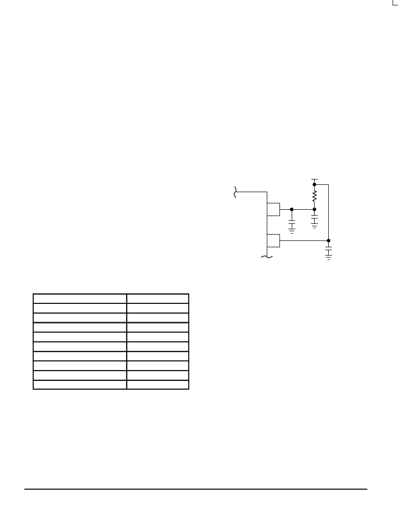
Figure 12. Power Supply Filter
VCCA
VCC
MPC972/973
0.01
μ
F
22
μ
F
0.01
μ
F
3.3V
RS=5–10
Figure 12 illustrates a typical power supply filter scheme.
The MPC972/973 is most susceptible to noise with spectral
content in the 1KHz to 1MHz range. Therefore the filter
should be designed to target this range. The key parameter
that needs to be met in the final filter design is the DC voltage
drop that will be seen between the VCC supply and the VCCA
pin of the MPC972/973. From the data sheet the IVCCA
current (the current sourced through the VCCA pin) is
typically 15mA (20mA maximum), assuming that a minimum
of 3.0V must be maintained on the VCCA pin very little DC
voltage drop can be tolerated when a 3.3V VCC supply is
used. The resistor shown in Figure 12 must have a
resistance of 5–10
to meet the voltage drop criteria. The RC
filter pictured will provide a broadband filter with
approximately 100:1 attenuation for noise whose spectral
content is above 20KHz. As the noise frequency crosses the
series resonant point of an individual capacitor it’s overall
impedance begins to look inductive and thus increases with
increasing frequency. The parallel capacitor combination
shown ensures that a low impedance path to ground exists
for frequencies well above the bandwidth of the PLL.
Although the MPC972/973 has several design features to
minimize the susceptibility to power supply noise (isolated
power and grounds and fully differential PLL) there still may
be applications in which overall performance is being
degraded due to system power supply noise. The power
supply filter schemes discussed in this section should be
相關(guān)PDF資料 |
PDF描述 |
|---|---|
| MPC974 | 3.3V PLL Clock Driver(3.3V PLL時(shí)鐘驅(qū)動(dòng)器) |
| MPC9774 | 3.3V / 2,5V 1:14 LVCMOS PLL CLOCK GENERATOR |
| MPC980 | Dual 3.3V PLL Clock Generator(雙3.3V PLL時(shí)鐘發(fā)生器) |
| MPC9855 | Clock Generator for PowerQUICC and PowerPC Microprocessors |
| MPC992 | Low Voltage PLL Clock Driver(低壓PLL時(shí)鐘驅(qū)動(dòng)器) |
相關(guān)代理商/技術(shù)參數(shù) |
參數(shù)描述 |
|---|---|
| MPC974 | 制造商:MOTOROLA 制造商全稱(chēng):Motorola, Inc 功能描述:LOW VOLTAGE PLL CLOCK DRIVER |
| MPC974A44 F44A WAF | 制造商:Motorola Inc 功能描述: |
| MPC9772 | 制造商:MOTOROLA 制造商全稱(chēng):Motorola, Inc 功能描述:3.3V 1:12 LVCMOS PLL Clock Generator |
| MPC9772AE | 功能描述:鎖相環(huán) - PLL 2.5 3.3V 250MHz Clock Generator RoHS:否 制造商:Silicon Labs 類(lèi)型:PLL Clock Multiplier 電路數(shù)量:1 最大輸入頻率:710 MHz 最小輸入頻率:0.002 MHz 輸出頻率范圍:0.002 MHz to 808 MHz 電源電壓-最大:3.63 V 電源電壓-最小:1.71 V 最大工作溫度:+ 85 C 最小工作溫度:- 40 C 封裝 / 箱體:QFN-36 封裝:Tray |
| MPC9772AER2 | 功能描述:時(shí)鐘發(fā)生器及支持產(chǎn)品 FSL 1-12 LVCMOS PLL Clock Generator, xta RoHS:否 制造商:Silicon Labs 類(lèi)型:Clock Generators 最大輸入頻率:14.318 MHz 最大輸出頻率:166 MHz 輸出端數(shù)量:16 占空比 - 最大:55 % 工作電源電壓:3.3 V 工作電源電流:1 mA 最大工作溫度:+ 85 C 安裝風(fēng)格:SMD/SMT 封裝 / 箱體:QFN-56 |
發(fā)布緊急采購(gòu),3分鐘左右您將得到回復(fù)。