- 您現(xiàn)在的位置:買賣IC網(wǎng) > PDF目錄3965 > MPC8323ECZQAFDC (Freescale Semiconductor)IC MPU PWRQUICC II 516-PBGA PDF資料下載
參數(shù)資料
| 型號: | MPC8323ECZQAFDC |
| 廠商: | Freescale Semiconductor |
| 文件頁數(shù): | 4/82頁 |
| 文件大?。?/td> | 0K |
| 描述: | IC MPU PWRQUICC II 516-PBGA |
| 產(chǎn)品培訓(xùn)模塊: | MPC8323E PowerQUICC II Pro Processor |
| 標(biāo)準(zhǔn)包裝: | 40 |
| 系列: | MPC83xx |
| 處理器類型: | 32-位 MPC83xx PowerQUICC II Pro |
| 速度: | 333MHz |
| 電壓: | 1V |
| 安裝類型: | 表面貼裝 |
| 封裝/外殼: | 516-BBGA |
| 供應(yīng)商設(shè)備封裝: | 516-FPBGA(27x27) |
| 包裝: | 托盤 |
| 配用: | MPC8323E-RDB-ND - BOARD REFERENCE DESIGN |
第1頁第2頁第3頁當(dāng)前第4頁第5頁第6頁第7頁第8頁第9頁第10頁第11頁第12頁第13頁第14頁第15頁第16頁第17頁第18頁第19頁第20頁第21頁第22頁第23頁第24頁第25頁第26頁第27頁第28頁第29頁第30頁第31頁第32頁第33頁第34頁第35頁第36頁第37頁第38頁第39頁第40頁第41頁第42頁第43頁第44頁第45頁第46頁第47頁第48頁第49頁第50頁第51頁第52頁第53頁第54頁第55頁第56頁第57頁第58頁第59頁第60頁第61頁第62頁第63頁第64頁第65頁第66頁第67頁第68頁第69頁第70頁第71頁第72頁第73頁第74頁第75頁第76頁第77頁第78頁第79頁第80頁第81頁第82頁
MPC8323E PowerQUICC II Pro Integrated Communications Processor Family Hardware Specifications, Rev. 4
12
Freescale Semiconductor
RESET Initialization
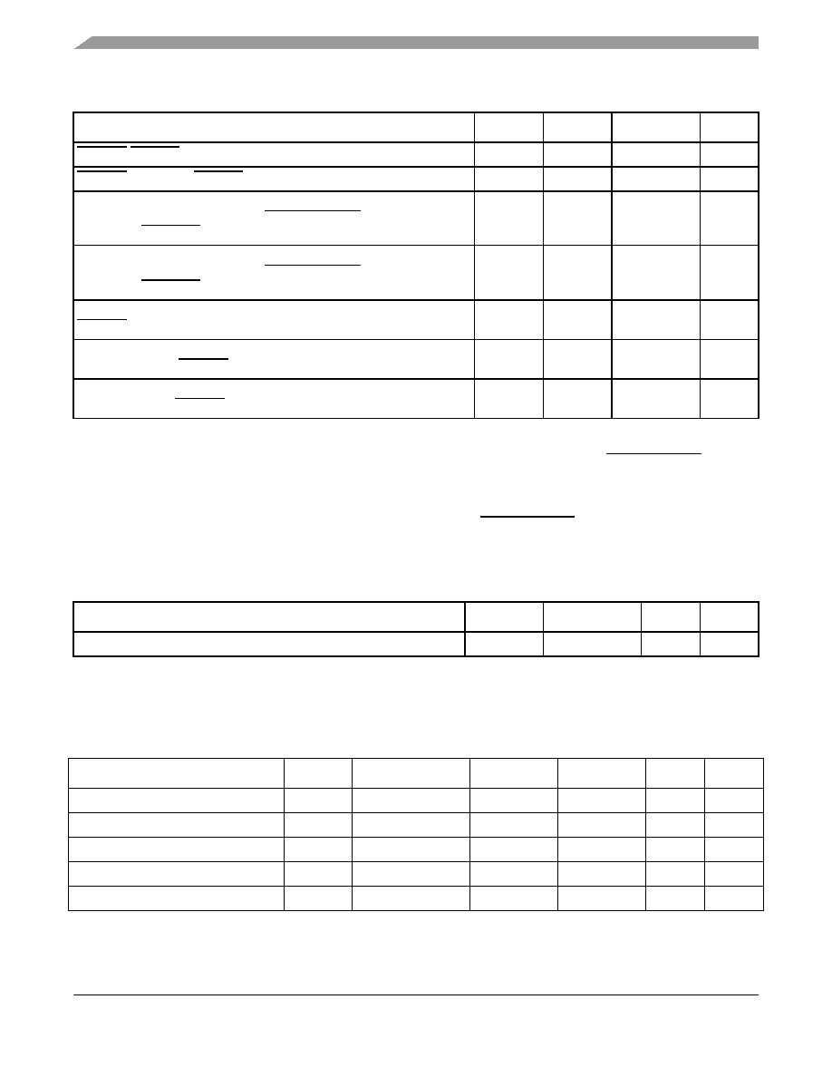
Table 10 provides the PLL lock times.
5.1
Reset Signals DC Electrical Characteristics
Table 11 provides the DC electrical characteristics for the MPC8323E reset signals mentioned in Table 9.
HRESET/SRESET assertion (output)
512
—
tPCI_SYNC_IN
1
HRESET negation to SRESET negation (output)
16
—
tPCI_SYNC_IN
1
Input setup time for POR configuration signals
(CFG_RESET_SOURCE[0:2] and CFG_CLKIN_DIV) with respect to
negation of PORESET when the MPC8323E is in PCI host mode
4—
tCLKIN
2
Input setup time for POR configuration signals
(CFG_RESET_SOURCE[0:2] and CFG_CLKIN_DIV) with respect to
negation of PORESET when the MPC8323E is in PCI agent mode
4—
tPCI_SYNC_IN
1
Input hold time for POR config signals with respect to negation of
HRESET
0—
ns
—
Time for the MPC8323E to turn off POR configuration signals with respect
to the assertion of HRESET
—4
ns
3
Time for the MPC8323E to turn on POR configuration signals with respect
to the negation of HRESET
1—
tPCI_SYNC_IN
1, 3
Notes:
1. tPCI_SYNC_IN is the clock period of the input clock applied to PCI_SYNC_IN. When the MPC8323E is In PCI host mode the
primary clock is applied to the CLKIN input, and PCI_SYNC_IN period depends on the value of CFG_CLKIN_DIV. See the
MPC8323E PowerQUICC II Pro Integrated Communications Processor Reference Manual for more details.
2. tCLKIN is the clock period of the input clock applied to CLKIN. It is only valid when the MPC8323E is in PCI host mode. See
the
MPC8323E PowerQUICC II Pro Integrated Communications Processor Reference Manual for more details.
3. POR configuration signals consists of CFG_RESET_SOURCE[0:2] and CFG_CLKIN_DIV.
Table 10. PLL Lock Times
Parameter/Condition
Min
Max
Unit
Notes
PLL lock times
—
100
μs—
Table 11. Reset Signals DC Electrical Characteristics
Characteristic
Symbol
Condition
Min
Max
Unit
Notes
Output high voltage
VOH
IOH = –6.0 mA
2.4
—
V
1
Output low voltage
VOL
IOL = 6.0 mA
—
0.5
V
1
Output low voltage
VOL
IOL = 3.2 mA
—
0.4
V
1
Input high voltage
VIH
—2.0
OVDD +0.3
V
1
Input low voltage
VIL
—
–0.3
0.8
V
—
Table 9. RESET Initialization Timing Specifications (continued)
Parameter/Condition
Min
Max
Unit
Notes
相關(guān)PDF資料 |
PDF描述 |
|---|---|
| IDT70V3589S133DR | IC SRAM 2MBIT 133MHZ 208QFP |
| MPC8323ECZQADDC | IC MPU PWRQUICC II 516-PBGA |
| IDT70V3589S133BCI | IC SRAM 2MBIT 133MHZ 256BGA |
| MPC8349ECZUAGDB | IC MPU PWRQUICC II 672-TBGA |
| IDT70V3399S133PRF | IC SRAM 2MBIT 133MHZ 128TQFP |
相關(guān)代理商/技術(shù)參數(shù) |
參數(shù)描述 |
|---|---|
| MPC8323ECZQAFDCA | 制造商:FREESCALE 制造商全稱:Freescale Semiconductor, Inc 功能描述:PowerQUICC? II Pro Integrated Communications Processor Family Hardware Specifications |
| MPC8323EEC | 制造商:FREESCALE 制造商全稱:Freescale Semiconductor, Inc 功能描述:PowerQUICC? II Pro Integrated Communications Processor Family Hardware Specifications |
| MPC8323E-MDS-PB | 功能描述:開發(fā)板和工具包 - 其他處理器 MPC8323E PROCESSOR BOARD RoHS:否 制造商:Freescale Semiconductor 產(chǎn)品:Development Systems 工具用于評估:P3041 核心:e500mc 接口類型:I2C, SPI, USB 工作電源電壓: |
| MPC8323E-RDB | 功能描述:開發(fā)板和工具包 - 其他處理器 REFERENCE DESIGN PQII PR RoHS:否 制造商:Freescale Semiconductor 產(chǎn)品:Development Systems 工具用于評估:P3041 核心:e500mc 接口類型:I2C, SPI, USB 工作電源電壓: |
| MPC8323E-RDB | 制造商:Freescale Semiconductor 功能描述:MPC8323E Integrated Multiservice Gateway |
發(fā)布緊急采購,3分鐘左右您將得到回復(fù)。