- 您現(xiàn)在的位置:買(mǎi)賣(mài)IC網(wǎng) > PDF目錄45312 > MCF54454VR266 (FREESCALE SEMICONDUCTOR INC) 32-BIT, 266 MHz, RISC PROCESSOR, PBGA360 PDF資料下載
參數(shù)資料
| 型號(hào): | MCF54454VR266 |
| 廠商: | FREESCALE SEMICONDUCTOR INC |
| 元件分類(lèi): | 微控制器/微處理器 |
| 英文描述: | 32-BIT, 266 MHz, RISC PROCESSOR, PBGA360 |
| 封裝: | 23 X 23 MM, ROHS COMPLIANT, TEPBGA-360 |
| 文件頁(yè)數(shù): | 9/48頁(yè) |
| 文件大小: | 945K |
| 代理商: | MCF54454VR266 |
第1頁(yè)第2頁(yè)第3頁(yè)第4頁(yè)第5頁(yè)第6頁(yè)第7頁(yè)第8頁(yè)當(dāng)前第9頁(yè)第10頁(yè)第11頁(yè)第12頁(yè)第13頁(yè)第14頁(yè)第15頁(yè)第16頁(yè)第17頁(yè)第18頁(yè)第19頁(yè)第20頁(yè)第21頁(yè)第22頁(yè)第23頁(yè)第24頁(yè)第25頁(yè)第26頁(yè)第27頁(yè)第28頁(yè)第29頁(yè)第30頁(yè)第31頁(yè)第32頁(yè)第33頁(yè)第34頁(yè)第35頁(yè)第36頁(yè)第37頁(yè)第38頁(yè)第39頁(yè)第40頁(yè)第41頁(yè)第42頁(yè)第43頁(yè)第44頁(yè)第45頁(yè)第46頁(yè)第47頁(yè)第48頁(yè)
Electrical Characteristics
MCF5445x ColdFire Microprocessor Data Sheet, Rev. 6
Freescale Semiconductor
17
5
Electrical Characteristics
This document contains electrical specification tables and reference timing diagrams for the MCF54455 microprocessor. This
section contains detailed information on DC/AC electrical characteristics and AC timing specifications.
The electrical specifications are preliminary and from previous designs or design simulations. These specifications may not be
fully tested or guaranteed at this early stage of the product life cycle. However, for production silicon, these specifications will
be met. Finalized specifications will be published after complete characterization and device qualifications have been
completed.
NOTE
The parameters specified in this MCU document supersede any values found in the module
specifications.
5.1
Absolute Maximum Ratings
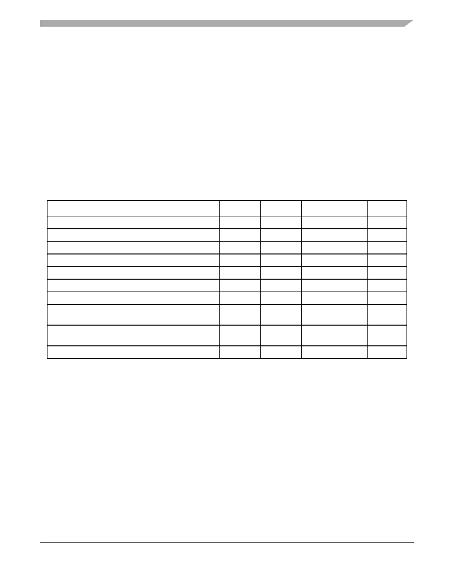
Table 5. Absolute Maximum Ratings1, 2
1 Functional operating conditions are given in Table 8. Absolute maximum ratings are stress ratings only, and functional
operation at the maximum is not guaranteed. Continued operation at these levels may affect device reliability or cause
permanent damage to the device.
2 This device contains circuitry protecting against damage due to high static voltage or electrical fields. However, it is
advised that normal precautions be taken to avoid application of any voltages higher than maximum-rated voltages to this
high-impedance circuit. Reliability of operation is enhanced if unused inputs are tied to an appropriate logic voltage level
(e.g., VSS or EVDD).
Rating
Symbol
Pin Name
Value
Units
External I/O pad supply voltage
EVDD
EVDD
-0.3 to +4.0
V
Internal oscillator supply voltage
OSCVDD
VDD_OSC
-0.3 to +4.0
V
Real-time clock supply voltage
RTCVDD
VDD_RTC
-0.5 to +2.0
V
Internal logic supply voltage
IVDD
IVDD
-0.5 to +2.0
V
SDRAM I/O pad supply voltage
SDVDD
SD_VDD
-0.3 to +4.0
V
PLL supply voltage
PVDD
VDD_A_PLL
-0.5 to +2.0
V
Digital input voltage3
3 Input must be current limited to the value specified. To determine the value of the required current-limiting resistor,
calculate resistance values for positive and negative clamp voltages, and then use the larger of the two values.
VIN
—
-0.3 to +3.6
V
Instantaneous maximum current
Single pin limit (applies to all pins) 3, 4, 5
4 All functional non-supply pins are internally clamped to V
SS and EVDD.
5 Power supply must maintain regulation within operating EV
DD range during instantaneous and operating maximum
current conditions. If positive injection current (Vin > EVDD) is greater than IDD, the injection current may flow out of EVDD
and could result in external power supply going out of regulation. Ensure the external EVDD load shunts current greater
than maximum injection current. This is the greatest risk when the MPU is not consuming power (ex; no clock). The power
supply must maintain regulation within operating EVDD range during instantaneous and operating maximum current
conditions.
IDD
—25
mA
Operating temperature range (packaged)
TA
(TL - TH)
—
-40 to +85
°C
Storage temperature range
Tstg
—
-55 to +150
°C
相關(guān)PDF資料 |
PDF描述 |
|---|---|
| MCF54451CVM180 | 32-BIT, 180 MHz, RISC PROCESSOR, PBGA256 |
| MCF54455VR266 | 32-BIT, 266 MHz, RISC PROCESSOR, PBGA360 |
| MCF54451VM240 | 32-BIT, 240 MHz, RISC PROCESSOR, PBGA256 |
| MCF54452CVR200 | 32-BIT, 200 MHz, RISC PROCESSOR, PBGA360 |
| MCF5471ZP200 | 32-BIT, 200 MHz, RISC PROCESSOR, PBGA388 |
相關(guān)代理商/技術(shù)參數(shù) |
參數(shù)描述 |
|---|---|
| MCF54455 | 制造商:FREESCALE 制造商全稱(chēng):Freescale Semiconductor, Inc 功能描述:ColdFire㈢ Microprocessor |
| MCF54455_08 | 制造商:FREESCALE 制造商全稱(chēng):Freescale Semiconductor, Inc 功能描述:ColdFire㈢ Microprocessor |
| MCF54455_0812 | 制造商:FREESCALE 制造商全稱(chēng):Freescale Semiconductor, Inc 功能描述:MCF5445x ColdFire?? Microprocessor Data Sheet |
| MCF54455_09 | 制造商:FREESCALE 制造商全稱(chēng):Freescale Semiconductor, Inc 功能描述:MCF5445x ColdFire?? Microprocessor Data Sheet |
| MCF54455ACVR200 | 制造商:Freescale Semiconductor 功能描述:MCF5445X RISC 32-BIT 200MHZ 1.8V/2.5V/3.3V 360-PIN TEBGA TRA - Trays |
發(fā)布緊急采購(gòu),3分鐘左右您將得到回復(fù)。