- 您現(xiàn)在的位置:買賣IC網(wǎng) > PDF目錄45312 > MCF54454VR266 (FREESCALE SEMICONDUCTOR INC) 32-BIT, 266 MHz, RISC PROCESSOR, PBGA360 PDF資料下載
參數(shù)資料
| 型號: | MCF54454VR266 |
| 廠商: | FREESCALE SEMICONDUCTOR INC |
| 元件分類: | 微控制器/微處理器 |
| 英文描述: | 32-BIT, 266 MHz, RISC PROCESSOR, PBGA360 |
| 封裝: | 23 X 23 MM, ROHS COMPLIANT, TEPBGA-360 |
| 文件頁數(shù): | 15/48頁 |
| 文件大小: | 945K |
| 代理商: | MCF54454VR266 |
第1頁第2頁第3頁第4頁第5頁第6頁第7頁第8頁第9頁第10頁第11頁第12頁第13頁第14頁當(dāng)前第15頁第16頁第17頁第18頁第19頁第20頁第21頁第22頁第23頁第24頁第25頁第26頁第27頁第28頁第29頁第30頁第31頁第32頁第33頁第34頁第35頁第36頁第37頁第38頁第39頁第40頁第41頁第42頁第43頁第44頁第45頁第46頁第47頁第48頁
MCF5445x ColdFire Microprocessor Data Sheet, Rev. 6
Electrical Characteristics
Freescale Semiconductor
22
5.6
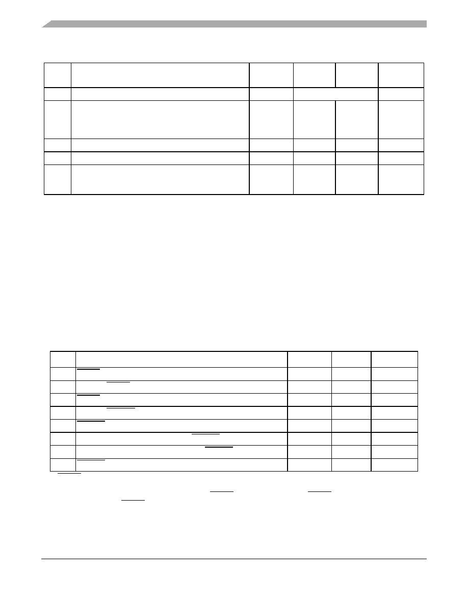
Reset Timing Specifications
12
Crystal capacitive load
CL
See crystal spec
13
Discrete load capacitance for XTAL
Discrete load capacitance for EXTAL
CL_XTAL
CL_EXTAL
—2
× (C
L -
CS_XTAL -
CS_EXTAL -
CS_PCB)
6
pF
14
Frequency un-LOCK Range
fUL
-4.0
4.0
% fsys
15
Frequency LOCK Range
fLCK
-2.0
2.0
% fsys
17
Peak-to-peak Jitter (Clock edge to clock edge)
Long Term Jitter
Cjitter
—
10
TBD
% FB_CLK
1 The minimum system frequency is the minimum input clock divided by the maximum low-power divider (16 MHz
÷ 32,768).
When the PLL is enabled, the minimum system frequency (fsys) is 150 MHz.
2
This parameter is guaranteed by characterization before qualification rather than 100% tested. Applies to external clock
reference only.
3
Proper PC board layout procedures must be followed to achieve specifications.
4
This parameter is guaranteed by design rather than 100% tested.
5
This specification is the PLL lock time only and does not include oscillator start-up time.
6
CS_PCB is the measured PCB stray capacitance on EXTAL and XTAL.
7
Jitter is the average deviation from the programmed frequency measured over the specified interval at maximum fsys.
Measurements are made with the device powered by filtered supplies and clocked by a stable external clock signal. Noise
injected into the PLL circuitry via PLL VDD, EVDD, and VSS and variation in crystal oscillator frequency increase the Cjitter
percentage for a given interval.
Table 11. Reset and Configuration Override Timing
Num
Characteristic
Min
Max
Unit
R11
1 RESET and Configuration Override data lines are synchronized internally. Setup and hold times must be met only if
recognition on a particular clock is required.
RESET valid to CLKIN (setup)
9
—
ns
R2
CLKIN to RESET invalid (hold)
1.5
—
ns
R3
RESET valid time2
2 During low power STOP, the synchronizers for the RESET input are bypassed and RESET is asserted asynchronously
to the system. Thus, RESET must be held a minimum of 100 ns.
5
—
CLKIN cycles
R4
CLKIN to RSTOUT valid
—
10
ns
R5
RSTOUT valid to Configuration Override inputs valid
0
—
ns
R6
Configuration Override inputs valid to RSTOUT invalid (setup)
20
—
CLKIN cycles
R7
Configuration Override inputs invalid after RSTOUT invalid (hold)
0
—
ns
R8
RSTOUT invalid to Configuration Override inputs High Impedance
—
1
CLKIN cycles
Table 10. PLL Electrical Characteristics (continued)
Num
Characteristic
Symbol
Min.
Value
Max.
Value
Unit
相關(guān)PDF資料 |
PDF描述 |
|---|---|
| MCF54451CVM180 | 32-BIT, 180 MHz, RISC PROCESSOR, PBGA256 |
| MCF54455VR266 | 32-BIT, 266 MHz, RISC PROCESSOR, PBGA360 |
| MCF54451VM240 | 32-BIT, 240 MHz, RISC PROCESSOR, PBGA256 |
| MCF54452CVR200 | 32-BIT, 200 MHz, RISC PROCESSOR, PBGA360 |
| MCF5471ZP200 | 32-BIT, 200 MHz, RISC PROCESSOR, PBGA388 |
相關(guān)代理商/技術(shù)參數(shù) |
參數(shù)描述 |
|---|---|
| MCF54455 | 制造商:FREESCALE 制造商全稱:Freescale Semiconductor, Inc 功能描述:ColdFire㈢ Microprocessor |
| MCF54455_08 | 制造商:FREESCALE 制造商全稱:Freescale Semiconductor, Inc 功能描述:ColdFire㈢ Microprocessor |
| MCF54455_0812 | 制造商:FREESCALE 制造商全稱:Freescale Semiconductor, Inc 功能描述:MCF5445x ColdFire?? Microprocessor Data Sheet |
| MCF54455_09 | 制造商:FREESCALE 制造商全稱:Freescale Semiconductor, Inc 功能描述:MCF5445x ColdFire?? Microprocessor Data Sheet |
| MCF54455ACVR200 | 制造商:Freescale Semiconductor 功能描述:MCF5445X RISC 32-BIT 200MHZ 1.8V/2.5V/3.3V 360-PIN TEBGA TRA - Trays |
發(fā)布緊急采購,3分鐘左右您將得到回復(fù)。