- 您現(xiàn)在的位置:買賣IC網(wǎng) > PDF目錄45312 > MCF54454VR266 (FREESCALE SEMICONDUCTOR INC) 32-BIT, 266 MHz, RISC PROCESSOR, PBGA360 PDF資料下載
參數(shù)資料
| 型號: | MCF54454VR266 |
| 廠商: | FREESCALE SEMICONDUCTOR INC |
| 元件分類: | 微控制器/微處理器 |
| 英文描述: | 32-BIT, 266 MHz, RISC PROCESSOR, PBGA360 |
| 封裝: | 23 X 23 MM, ROHS COMPLIANT, TEPBGA-360 |
| 文件頁數(shù): | 30/48頁 |
| 文件大小: | 945K |
| 代理商: | MCF54454VR266 |
第1頁第2頁第3頁第4頁第5頁第6頁第7頁第8頁第9頁第10頁第11頁第12頁第13頁第14頁第15頁第16頁第17頁第18頁第19頁第20頁第21頁第22頁第23頁第24頁第25頁第26頁第27頁第28頁第29頁當(dāng)前第30頁第31頁第32頁第33頁第34頁第35頁第36頁第37頁第38頁第39頁第40頁第41頁第42頁第43頁第44頁第45頁第46頁第47頁第48頁
MCF5445x ColdFire Microprocessor Data Sheet, Rev. 6
Electrical Characteristics
Freescale Semiconductor
36
5.15
ATA Interface Timing Specifications
The ATA controller is compatible with the ATA/ATAPI-6 industry standard. Refer to the ATA/ATAPI-6 Specficiation and the
ATA controller chapter of the MCF54455 Reference Manual for timing diagrams of the various modes of operation.
The timings of the various ATA data transfer modes are determined by a set of timing equations described in the ATA section
of the MCF54455 Reference Manual. These timing equations must be fulfilled for the ATA host to meet timing. Table 25
provides implementation specific timing parameters necessary to complete the timing equations.
5.16
DSPI Timing Specifications
The DMA Serial Peripheral Interface (DSPI) provides a synchronous serial bus with master and slave operations. Many of the
transfer attributes are programmable. Table 26 provides DSPI timing characteristics for classic SPI timing modes. Refer to the
DSPI chapter of the MCF54455 Reference Manual for information on the modified transfer formats used for communicating
with slower peripheral devices.
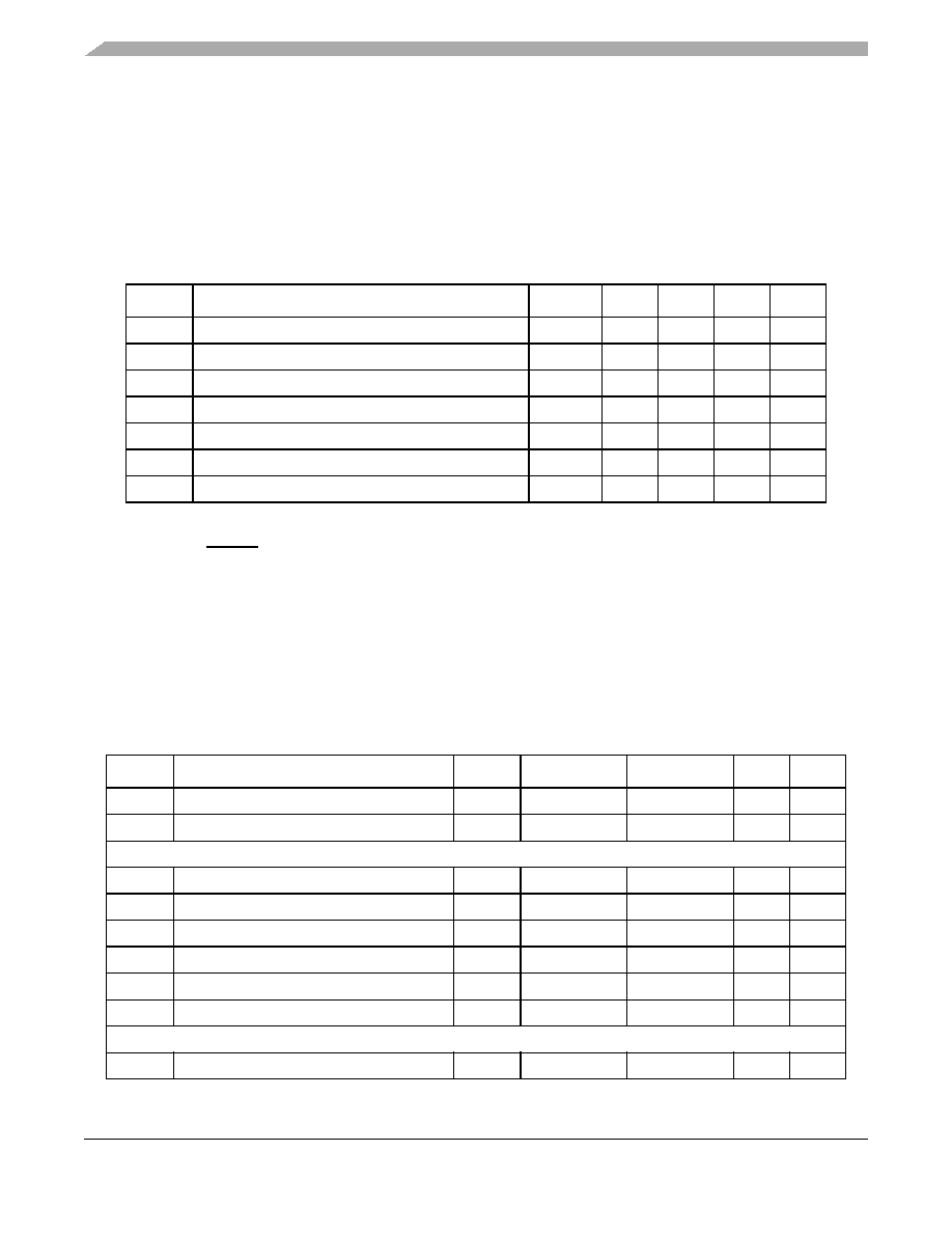
Table 25. ATA Interface Timing Specifications1,2
1 These parameters are guaranteed by design and not testable.
2 All timings specified with a capacitive load of 40pF.
Name
Characteristic
Symbol
Min
Max
Unit
Notes
A1
Setup time — ATA_IORDY to SYSCLK falling
tSUI
4.0
—
ns
A2
Hold time — ATA_IORDY from SYSCLK falling
tHI
3.0
—
ns
A3
Setup time — ATA_DATA[15:0] to SYSCLK rising
tSU
4.0
—
ns
A4
Propagation delay — SYSCLK rising to all outputs
tCO
—7.0
ns
3
3 Applies to ATA_CS[1:0], ATA_DA[2:0], ATA_DIOR, ATA_DIOW, ATA_DMACK, ATA_DATA[15:0]
A5
Output skew
tSKEW1
—1.5
ns
A6
Setup time — ATA_DATA[15:0] valid to ATA_IORDY
tI_DS
2.0
—
ns
4
4 Applies to Ultra DMA data-in burst only
A7
Hold time — ATA_IORDY to ATA_DATA[15:0] invalid
tI_DH
3.5
—
ns
Table 26. DSPI Module AC Timing Specifications1
Name
Characteristic
Symbol
Min
Max
Unit
Notes
DS1
DSPI_SCK Cycle Time
tSCK
4 x tSYS
—ns
2
DS2
DSPI_SCK Duty Cycle
—
(tsck ÷ 2) - 2.0
(tsck ÷ 2) + 2.0
ns
3
Master Mode
DS3
DSPI_PCSn to DSPI_SCK delay
tCSC
(2
× t
SYS) - 1.5
—
ns
4
DS4
DSPI_SCK to DSPI_PCSn delay
tASC
(2
× t
SYS) - 3.0
—
ns
5
DS5
DSPI_SCK to DSPI_SOUT valid
—
5
ns
DS6
DSPI_SCK to DSPI_SOUT invalid
—
-5
—
ns
DS7
DSPI_SIN to DSPI_SCK input setup
—
9
—
ns
DS8
DSPI_SCK to DSPI_SIN input hold
—
0
—
ns
Slave Mode
DS9
DSPI_SCK to DSPI_SOUT valid
—
10
ns
相關(guān)PDF資料 |
PDF描述 |
|---|---|
| MCF54451CVM180 | 32-BIT, 180 MHz, RISC PROCESSOR, PBGA256 |
| MCF54455VR266 | 32-BIT, 266 MHz, RISC PROCESSOR, PBGA360 |
| MCF54451VM240 | 32-BIT, 240 MHz, RISC PROCESSOR, PBGA256 |
| MCF54452CVR200 | 32-BIT, 200 MHz, RISC PROCESSOR, PBGA360 |
| MCF5471ZP200 | 32-BIT, 200 MHz, RISC PROCESSOR, PBGA388 |
相關(guān)代理商/技術(shù)參數(shù) |
參數(shù)描述 |
|---|---|
| MCF54455 | 制造商:FREESCALE 制造商全稱:Freescale Semiconductor, Inc 功能描述:ColdFire㈢ Microprocessor |
| MCF54455_08 | 制造商:FREESCALE 制造商全稱:Freescale Semiconductor, Inc 功能描述:ColdFire㈢ Microprocessor |
| MCF54455_0812 | 制造商:FREESCALE 制造商全稱:Freescale Semiconductor, Inc 功能描述:MCF5445x ColdFire?? Microprocessor Data Sheet |
| MCF54455_09 | 制造商:FREESCALE 制造商全稱:Freescale Semiconductor, Inc 功能描述:MCF5445x ColdFire?? Microprocessor Data Sheet |
| MCF54455ACVR200 | 制造商:Freescale Semiconductor 功能描述:MCF5445X RISC 32-BIT 200MHZ 1.8V/2.5V/3.3V 360-PIN TEBGA TRA - Trays |
發(fā)布緊急采購,3分鐘左右您將得到回復(fù)。