- 您現(xiàn)在的位置:買賣IC網(wǎng) > PDF目錄9833 > MAX3301EETJ+T (Maxim Integrated Products)IC USB TXRX OTG 32-TQFN-EP PDF資料下載
參數(shù)資料
| 型號: | MAX3301EETJ+T |
| 廠商: | Maxim Integrated Products |
| 文件頁數(shù): | 38/38頁 |
| 文件大小: | 0K |
| 描述: | IC USB TXRX OTG 32-TQFN-EP |
| 產(chǎn)品培訓(xùn)模塊: | Lead (SnPb) Finish for COTS Obsolescence Mitigation Program |
| 標(biāo)準(zhǔn)包裝: | 2,500 |
| 類型: | 收發(fā)器 |
| 規(guī)程: | USB 2.0 |
| 電源電壓: | 3 V ~ 4.5 V |
| 安裝類型: | 表面貼裝 |
| 封裝/外殼: | 32-WFQFN 裸露焊盤 |
| 供應(yīng)商設(shè)備封裝: | 32-TQFN-EP(5x5) |
| 包裝: | 帶卷 (TR) |
第1頁第2頁第3頁第4頁第5頁第6頁第7頁第8頁第9頁第10頁第11頁第12頁第13頁第14頁第15頁第16頁第17頁第18頁第19頁第20頁第21頁第22頁第23頁第24頁第25頁第26頁第27頁第28頁第29頁第30頁第31頁第32頁第33頁第34頁第35頁第36頁第37頁當(dāng)前第38頁
MAX3301E/MAX3302E
USB On-the-Go Transceivers and Charge Pumps
_______________________________________________________________________________________
9
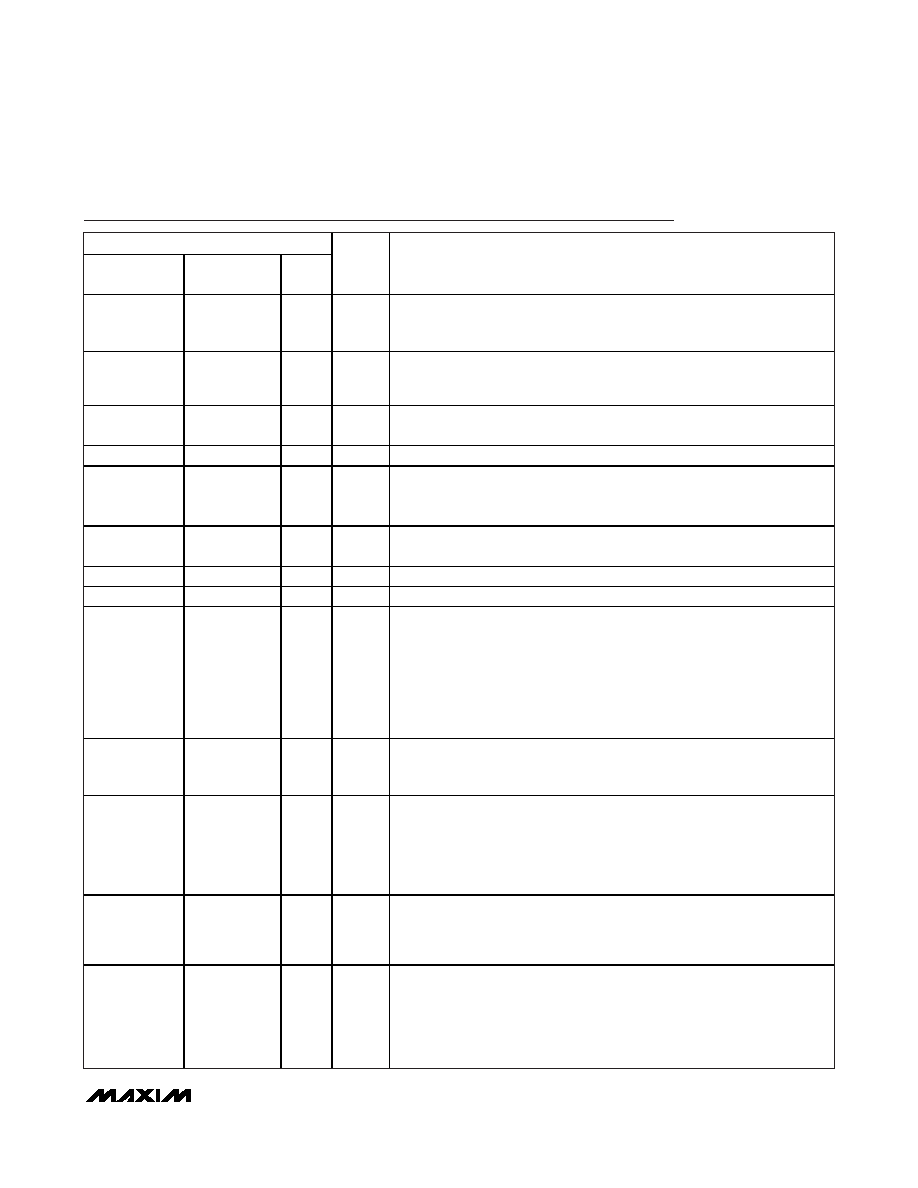
Pin Description
PIN
MAX3302E
28-PIN TQFN
MAX3301E
32-PIN TQFN
UCSP/
WLP
NAME
FUNCTION
1
2
D2
DAT_VP
System-Side Data Input/Output. DAT_VP is an input if
OE/INT is logic 0.
DAT_VP is an output if
OE/INT is logic 1. Program the function of DAT_VP
with the dat_se0 bit (bit 2 of control register 1, see Table 7).
2, 25
3, 29
D1, E3
VCC
Input Power Supply. Connect a +3V to +4.5V supply to VCC and bypass to
GND with a 1F capacitor. The supply range enables direct powering from
one Li+ battery.
3, 9, 23
1, 4, 9, 12, 17,
25, 28
—
N.C.
No Connection. Not internally connected.
4
5
C1
C-
Charge-Pump Flying-Capacitor Negative Terminal
5
6
C2
SE0_VM
System-Side Data Input/Output. SE0_VM is an input if
OE/INT is logic 0.
SE0_VM is an output if
OE/INT is logic 1. Program the function of SE0_VM
with the dat_se0 bit (bit 2 of control register 1, see Table 7).
6, 18
7, 21
B1, C5
GND
Ground
7
8
A1
SDA
I2C-Compatible Serial Data Interface. Open-drain data input/output.
8
10
B2
SCL
I2C-Compatible Serial Clock Input
10
11
A2
OE/INT
Output Enable.
OE/INT controls the input or output status of DAT_VP/SE0_VM
and D+/D-. When
OE/INT is logic 0, the device is in transmit mode. When
OE/INT is logic 1, the device is in receive mode. When in suspend mode,
OE/INT can be programmed to function as an interrupt output that detects the
same interrupts as
INT. The oe_int_en bit (bit 5 of control register 1, see Table
7) enables and disables the interrupt circuitry of
OE/INT. The irq_mode bit (bit 1
of special-function register 2, see Table 15) programs the output configuration
of
INT and OE/INT as open-drain or push-pull.
11
13
A3
RCV
D+ and D- Differential Receiver Output. In receive mode (see Table 4), when
D+ is high and D- is low, RCV is high. In receive mode, when D+ is low and
D- is high, RCV is low. RCV is low in suspend mode.
12
14
B3
SPD
Speed-Selector Input. Connect SPD to GND to select the low-speed data rate
(1.5Mbps). Connect SPD to VL to select the full-speed data rate (12Mbps).
Disable the SPD input by writing a 1 to spd_susp_ctl (bit 1 in special-function
register 1, see Table 14). The speed bit (bit 0 of control register 1, see Table
7) determines the maximum data rate of the MAX3301E/MAX3302E when the
SPD input is disabled.
13
15
A4
VL
System-Side Logic-Supply Input. Connect to the system’s logic-level power
supply, +1.65V to +3.6V. This sets the maximum output levels of the logic
outputs and the input thresholds of the logic inputs. Bypass to GND with a
0.1F capacitor.
14
16
A5
SUS
Active-High Suspend Input. Drive SUS low for normal USB operation. Drive
SUS high to enable suspend mode. RCV asserts low in suspend mode.
Disable the SUS input by writing a 1 to spd_susp_ctl (bit 1 in special-function
register 1, see Table 14). The suspend bit (bit 1 of control register 1, see
Table 7) determines the operating mode of the MAX3301E/MAX3302E when
the SUS input is disabled.
相關(guān)PDF資料 |
PDF描述 |
|---|---|
| MS27473T16A8PA | CONN PLUG 8POS STRAIGHT W/PINS |
| MAX13081EASA+T | IC TXRX RS485/RS422 8-SOIC |
| MX574AKEQI+T | IC ADC 12BIT W/REF 28-PLCC |
| MAX3040ESE+T | IC RS485/422 TRANS QUAD 16-SOIC |
| MX7572KEWG12+ | IC ADC 12BIT HS 24-SOIC |
相關(guān)代理商/技術(shù)參數(shù) |
參數(shù)描述 |
|---|---|
| MAX3301EEWA+ | 制造商:Maxim Integrated Products 功能描述:USB ON-THE-GO TRANSCEIVERS AND CHARGE PUMPS - Rail/Tube |
| MAX3301EEWA+T | 制造商:Maxim Integrated Products 功能描述:USB ON-THE-GO TRANSCEIVER AND CHARGE PUMP - Tape and Reel 制造商:Maxim Integrated Products 功能描述:IC USB TXRX OTG WLP |
| MAX3302EEBA | 制造商:Maxim Integrated Products 功能描述:USB ON-THE-GO TRANSCEIVER AND CHARG - Rail/Tube |
| MAX3302EEBA+ | 制造商:Maxim Integrated Products 功能描述:USB ON-THE-GO TRANSCEIVERS AND CHARGE PUMPS - Rail/Tube |
| MAX3302EEBA+T | 制造商:Maxim Integrated Products 功能描述:USB ON-THE-GO TRANSCEIVERS AND CHARGE PUMPS - Tape and Reel |
發(fā)布緊急采購,3分鐘左右您將得到回復(fù)。