- 您現(xiàn)在的位置:買賣IC網(wǎng) > PDF目錄180243 > M7A3PE600-FFG256I FPGA, 600000 GATES, PBGA256 PDF資料下載
參數(shù)資料
| 型號: | M7A3PE600-FFG256I |
| 元件分類: | FPGA |
| 英文描述: | FPGA, 600000 GATES, PBGA256 |
| 封裝: | 1 MM PITCH, FBGA-256 |
| 文件頁數(shù): | 128/168頁 |
| 文件大小: | 1335K |
| 代理商: | M7A3PE600-FFG256I |
第1頁第2頁第3頁第4頁第5頁第6頁第7頁第8頁第9頁第10頁第11頁第12頁第13頁第14頁第15頁第16頁第17頁第18頁第19頁第20頁第21頁第22頁第23頁第24頁第25頁第26頁第27頁第28頁第29頁第30頁第31頁第32頁第33頁第34頁第35頁第36頁第37頁第38頁第39頁第40頁第41頁第42頁第43頁第44頁第45頁第46頁第47頁第48頁第49頁第50頁第51頁第52頁第53頁第54頁第55頁第56頁第57頁第58頁第59頁第60頁第61頁第62頁第63頁第64頁第65頁第66頁第67頁第68頁第69頁第70頁第71頁第72頁第73頁第74頁第75頁第76頁第77頁第78頁第79頁第80頁第81頁第82頁第83頁第84頁第85頁第86頁第87頁第88頁第89頁第90頁第91頁第92頁第93頁第94頁第95頁第96頁第97頁第98頁第99頁第100頁第101頁第102頁第103頁第104頁第105頁第106頁第107頁第108頁第109頁第110頁第111頁第112頁第113頁第114頁第115頁第116頁第117頁第118頁第119頁第120頁第121頁第122頁第123頁第124頁第125頁第126頁第127頁當(dāng)前第128頁第129頁第130頁第131頁第132頁第133頁第134頁第135頁第136頁第137頁第138頁第139頁第140頁第141頁第142頁第143頁第144頁第145頁第146頁第147頁第148頁第149頁第150頁第151頁第152頁第153頁第154頁第155頁第156頁第157頁第158頁第159頁第160頁第161頁第162頁第163頁第164頁第165頁第166頁第167頁第168頁
ProASIC3E Flash Family FPGAs
2- 50
Advanced v0.5
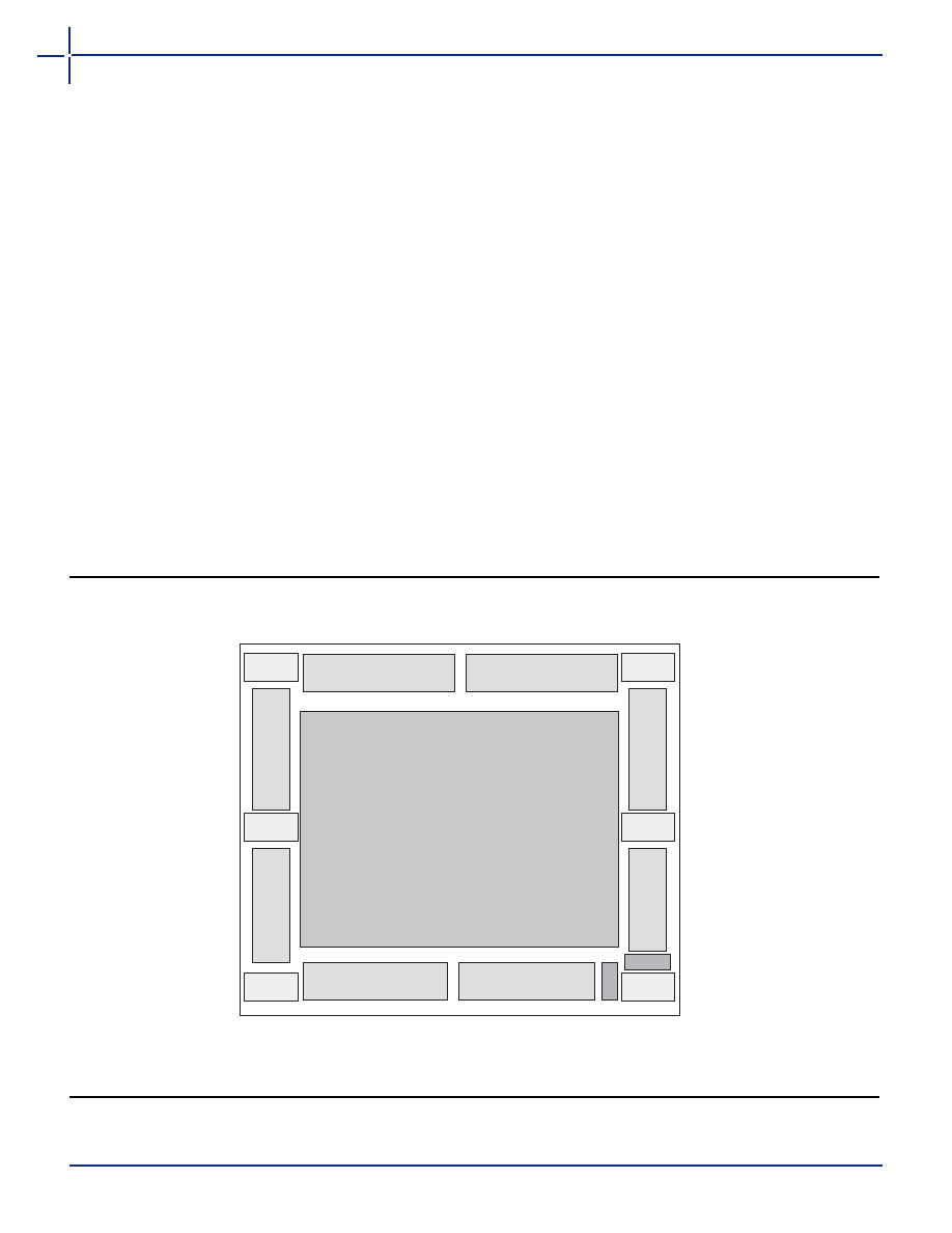
User I/O Naming Convention
Due to the comprehensive and flexible nature of ProASIC3E device user I/Os, a naming scheme is used to show the
details of the I/O (Figure 2-36). The name identifies to which I/O bank it belongs, as well as the pairing and pin polarity
for differential I/Os.
I/O Nomenclature = Gmn/IOuxwByVz
Gmn is only used for I/Os that also have CCC access—i.e., global pins.
G
= Global
m
= Global pin location associated with each CCC on the device: A (northwest corner), B (northeast corner), C (east
middle), D (southeast corner), E (southwest corner), and F (west middle)
n
= Global input MUX and pin number of the associated Global location m, either A0, A1,A2, B0, B1, B2, C0, C1, or
C2. Figure 2-14 on page 2-16 shows the three input pins per each clock source MUX at the CCC location m.
u
= I/O pair number in the bank, starting at 00 from the northwest I/O bank and proceeds in a clockwise direction.
x
= P (Positive) or N (Negative) for differential pairs, or R (Regular—single-ended) for the I/Os that support single-
ended and voltage-referenced I/O standards only.
w
= D (Differential Pair) or P (Pair) or S (Single-Ended). D (Differential Pair) if both members of the pair are bonded
out to adjacent pins or are separated only by one GND or NC pin; P (Pair) if both members of the pair are
bonded out but do not meet the adjacency requirement; or S (Single-Ended) if the I/O pair is not bonded out.
For Differential (D) pairs, adjacency for ball grid packages means only vertical or horizontal. Diagonal
adjacency does not meet the requirements for a true differential pair.
B
= Bank
y
= Bank number [0..7]. The bank number starts at 0 from northwest I/O bank and proceeds in a clockwise direction.
V
= VREF
z
= VREF minibank number [0...4]. A given voltage-referenced signal spans 16 pins (typically) in an I/O bank. Voltage
banks may have multiple VREF minibanks.
Figure 2-36 User I/O Naming Conventions of ProASIC3E Devices
A3PE600
CCC/PLL
“F”
CCC/PLL
“C”
CCC/PLL
“D”
CCC/PLL
“B”
CCC/PLL
“A”
CCC/PLL
“E”
Bank 0
Bank 1
Bank 5
Bank 4
JT
A
G
Ba
n
k
3
Ba
n
k
2
JTAG
Ba
n
k
6
Ba
n
k
7
A3PE600
CCC/PLL
“F”
CCC/PLL
“C”
CCC/PLL
“D”
CCC/PLL
“B”
CCC/PLL
“A”
CCC/PLL
“E”
Bank 0
Bank 1
Bank 5
Bank 4
JT
A
G
Ba
n
k
3
Ba
n
k
2
JTAG
Ba
n
k
6
Ba
n
k
7
A3PE600
A3PE1500
A3PE3000
CCC/PLL
'A'
Bank 0
Bank 1
Bank 5
Bank 4
JT
A
G
Ba
n
k
3
Ba
n
k
2
JTAG
Ba
n
k
6
Ba
n
k
7
CCC/PLL
'F'
CCC/PLL
'E'
CCC/PLL
'D'
CCC/PLL
'C'
CCC/PLL
'B'
GNDQ
VMV7
VMV6
GNDQ
VMV
0
G
NDQ
GN
D
GN
D
G
NDQ
VMV
1
VM
V4
TM
S
TD
I
TC
K
GN
D
Q
GN
D
GN
D
GN
D
Q
VM
V5
V
CC
V
CC
V
COMPLF
V
CCPLF
V
COMPLE
V
CCPLE
V
COMPLA
V
CCPLA
GND
V
CCIB7
V
CCIB6
GND
V
CC
V
CC
V
CCI
B0
V
CC
V
CCI
B1
V
CC
V
CCI
B4
V
CCI
B5
V
CC
GNDQ
VMV2
GND
TRST
TDO
VMV3
GNDQ
V
COMPLB
V
COMPLC
V
CCPLB
V
CCPLC
V
JTAG
V
CC
V
CC
V
COMPLD
V
PUMP
V
CCPLD
V
CCIB2
GND
V
CC
V
CCIB3
相關(guān)PDF資料 |
PDF描述 |
|---|---|
| M7A3PE600-FFG484I | FPGA, 600000 GATES, PBGA484 |
| M7A3PE600-FFGG256I | FPGA, 600000 GATES, PBGA256 |
| M7A3PE600-FFGG484I | FPGA, 600000 GATES, PBGA484 |
| M7A3PE600-FPQ208I | FPGA, 600000 GATES, PQFP208 |
| M7A3PE600-FPQG208I | FPGA, 600000 GATES, PQFP208 |
相關(guān)代理商/技術(shù)參數(shù) |
參數(shù)描述 |
|---|---|
| M7A5 | 制造商:未知廠家 制造商全稱:未知廠家 功能描述:MEDIUM CURRENT SILICON RECTIFIERS |
| M7A9 | 制造商:未知廠家 制造商全稱:未知廠家 功能描述:MEDIUM CURRENT SILICON RECTIFIERS |
| M7AFS600-1FG256 | 制造商:Microsemi Corporation 功能描述:FPGA FUSION 600K GATES 1282.05MHZ 130NM 1.5V 256FBGA - Trays 制造商:Microsemi SOC Products Group 功能描述:FPGA FUSION 600K GATES 1282.05MHZ 130NM 1.5V 256FBGA - Trays |
| M7AFS600-1FG256ES | 制造商:ACTEL 制造商全稱:Actel Corporation 功能描述:Actel Fusion Mixed-Signal FPGAs |
| M7AFS600-1FG256I | 制造商:Microsemi Corporation 功能描述:FPGA FUSION 600K GATES 1282.05MHZ 130NM 1.5V 256FBGA - Trays 制造商:Microsemi SOC Products Group 功能描述:FPGA FUSION 600K GATES 1282.05MHZ 130NM 1.5V 256FBGA - Trays |
發(fā)布緊急采購,3分鐘左右您將得到回復(fù)。