- 您現(xiàn)在的位置:買賣IC網(wǎng) > PDF目錄1924 > IDT82P2828BHG (IDT, Integrated Device Technology Inc)IC LIU T1/J1/E1 28+1CH 640-PBGA PDF資料下載
參數(shù)資料
| 型號: | IDT82P2828BHG |
| 廠商: | IDT, Integrated Device Technology Inc |
| 文件頁數(shù): | 68/154頁 |
| 文件大?。?/td> | 0K |
| 描述: | IC LIU T1/J1/E1 28+1CH 640-PBGA |
| 標準包裝: | 5 |
| 類型: | 線路接口裝置(LIU) |
| 規(guī)程: | E1 |
| 電源電壓: | 3.13 V ~ 3.47 V |
| 安裝類型: | 表面貼裝 |
| 封裝/外殼: | 640-BGA 裸露焊盤 |
| 供應(yīng)商設(shè)備封裝: | 640-PBGA-EP(31x31) |
| 包裝: | 托盤 |
| 其它名稱: | 82P2828BHG |
第1頁第2頁第3頁第4頁第5頁第6頁第7頁第8頁第9頁第10頁第11頁第12頁第13頁第14頁第15頁第16頁第17頁第18頁第19頁第20頁第21頁第22頁第23頁第24頁第25頁第26頁第27頁第28頁第29頁第30頁第31頁第32頁第33頁第34頁第35頁第36頁第37頁第38頁第39頁第40頁第41頁第42頁第43頁第44頁第45頁第46頁第47頁第48頁第49頁第50頁第51頁第52頁第53頁第54頁第55頁第56頁第57頁第58頁第59頁第60頁第61頁第62頁第63頁第64頁第65頁第66頁第67頁當前第68頁第69頁第70頁第71頁第72頁第73頁第74頁第75頁第76頁第77頁第78頁第79頁第80頁第81頁第82頁第83頁第84頁第85頁第86頁第87頁第88頁第89頁第90頁第91頁第92頁第93頁第94頁第95頁第96頁第97頁第98頁第99頁第100頁第101頁第102頁第103頁第104頁第105頁第106頁第107頁第108頁第109頁第110頁第111頁第112頁第113頁第114頁第115頁第116頁第117頁第118頁第119頁第120頁第121頁第122頁第123頁第124頁第125頁第126頁第127頁第128頁第129頁第130頁第131頁第132頁第133頁第134頁第135頁第136頁第137頁第138頁第139頁第140頁第141頁第142頁第143頁第144頁第145頁第146頁第147頁第148頁第149頁第150頁第151頁第152頁第153頁第154頁
IDT82P2828
28(+1) CHANNEL HIGH-DENSITY T1/E1/J1 LINE INTERFACE UNIT
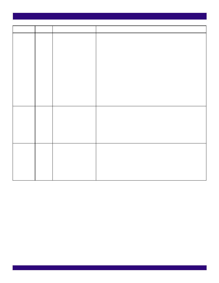
Pin Description
20
February 6, 2009
RCLKn / RMFn
(n=0~28)
Output
AK10, AD2, AE4, AH2, AK4, AH5,
AK7, AH8, AH20, AK22, AH23,
AK25, AH26, AK28, AG29, A28,
A26, C25, A23, C22, A20, C19,
A17, C16, B14, D13, B11, D10, B8
RCLKn: Receive Clock for Channel 0 ~ 28
When the receive system interface is configured to Single Rail NRZ Format mode, Dual Rail
NRZ Format mode or Dual Rail RZ Format mode, this multiplex pin is used as RCLKn.
RCLKn outputs a 1.544 MHz (in T1/J1 mode) or 2.048 MHz (in E1 mode) clock which is
recovered from the received signal.
The data output on RDn and RMFn (in Receive Single Rail NRZ Format mode) or RDPn/
RDNn (in Receive Dual Rail NRZ Format mode, Receive Dual Rail RZ Format mode and
Receive Dual Rail Sliced) is updated on the active edge of RCLKn. The active edge is
selected by the RCK_ES bit (b4, RCF1,...).
In LLOS condition, RCLKn output high or XCLK,
as selected by the RCKH bit (b7,
,...) (refer to Section 3.5.3.1 Line LOS (LLOS) for details).
When the receiver is powered down, RCLKn will be in High-Z state or low, as selected by the
RHZ bit (b6, RCF0,...).
RMFn: Receive Multiplex Function for Channel 0 ~ 28
When the receive system interface is configured to Dual Rail Sliced mode, this multiplex pin is
used as RMFn.
(Refer to the description of RMFn of the RDNn/RMFn multiplex pin for details).
LLOS
Output
AF17
LLOS: Receive Line Loss Of Signal
LLOS synchronizes with the output of CLKE1 and can indicate the LLOS (Line LOS) status of
all 29 channels in a serial format.
When the clock output on CLKE1 is enabled, LLOS indicates the LLOS status of the 29 chan-
nels in a serial format and repeats every twenty-nine cycles. Channel 0 is positioned by
LLOS0. Refer to the description of LLOS0 below for details.
LLOS is updated on the rising edge of CLKE1 and is always active high.
When the clock output of CLKE1 is disabled, LLOS will be held in High-Z state.
(Refer to Section 3.5.3.1 Line LOS (LLOS) for details.)
LLOS0
Output
AF18
LLOS0: Receive Line Loss Of Signal for Channel 0
LLOS0 can indicate the position of channel 0 on the LLOS pin.
When the clock output on CLKE1 is enabled, LLOS0 pulses high for one CLKE1 clock cycle to
indicate the position of channel 0 on the LLOS pin. When CLKE1 outputs 8 KHz clock, LLOS0
pulses high for one 8 KHz clock cycle (125 s) every twenty-nine 8 KHz clock cycles; when
CLKE1 outputs 2.048 MHz clock, LLOS0 pulses high for one 2.048 MHz clock cycle (488 ns)
every twenty-nine 2.048 MHz clock cycles. LLOS0 is updated on the rising edge of CLKE1.
When the clock output on CLKE1 is disabled, LLOS0 will be held in High-Z state.
(Refer to Section 3.5.3.1 Line LOS (LLOS) for details.)
Name
I / O
Pin No.
Description
相關(guān)PDF資料 |
PDF描述 |
|---|---|
| IDT82P2916BFG | IC LIU T1/E1/J1 16CH SH 484BGA |
| IDT82P5088BBG | IC LIU T1/E1/J1 OCTAL 256PBGA |
| IDT82V2041EPPG | IC LIU T1/J1/E1 1CH 44-TQFP |
| IDT82V2042EPFG | IC LIU T1/J1/E1 2CH SHORT 80TQFP |
| IDT82V2044EPFG | IC LIU T1/E1 QUAD SHORT 128-TQFP |
相關(guān)代理商/技術(shù)參數(shù) |
參數(shù)描述 |
|---|---|
| IDT82P2916 | 制造商:IDT 制造商全稱:Integrated Device Technology 功能描述:16-Channel High-Density T1/E1/J1 Line Interface Unit |
| IDT82P2916BFG | 功能描述:IC LIU T1/E1/J1 16CH SH 484BGA RoHS:是 類別:集成電路 (IC) >> 接口 - 電信 系列:- 產(chǎn)品培訓模塊:Lead (SnPb) Finish for COTS 產(chǎn)品變化通告:Product Discontinuation 06/Feb/2012 標準包裝:750 系列:* |
| IDT82P2916BFG8 | 制造商:Integrated Device Technology Inc 功能描述:IC LIU T1/E1/J1 16CH SH 484BGA |
| IDT82P5088 | 制造商:IDT 制造商全稱:Integrated Device Technology 功能描述:Universal Octal T1/E1/J1 LIU with Integrated Clock Adapter |
| IDT82P5088BBBLANK | 制造商:IDT 制造商全稱:Integrated Device Technology 功能描述:Universal Octal T1/E1/J1 LIU with Integrated Clock Adapter |
發(fā)布緊急采購,3分鐘左右您將得到回復。