- 您現(xiàn)在的位置:買賣IC網(wǎng) > PDF目錄379806 > CD40105BMS (Intersil Corporation) CMOS FIFO Register(CMOS 先進先出寄存器) PDF資料下載
參數(shù)資料
| 型號: | CD40105BMS |
| 廠商: | Intersil Corporation |
| 英文描述: | CMOS FIFO Register(CMOS 先進先出寄存器) |
| 中文描述: | FIFO寄存器的CMOS的CMOS(先進先出寄存器) |
| 文件頁數(shù): | 2/10頁 |
| 文件大小: | 116K |
| 代理商: | CD40105BMS |
7-1318
CD40105BMS
Unloading Data
- As soon as the first word has rippled to
the output, DATA-OUT READY (DOR) goes high, and data
can be removed by a falling edge on the SO input. This fall-
ing edge causes the DOR signal to go low while the word on
the output is dumped and the next word moves to the output.
As long as valid data are available in the FIFO, the DOR sig-
nal will go high again signifying that the next word is ready at
the output. When the FIFO is empty, DOR will remain low,
and any further commands will be ignored until a “1” marker
ripples down to the last control register, when DOR goes
high. Unloading of data is inhibited while the 3-state control
input is high. The 3-state control signal should not be shifted
from high to low (data outputs turned on) while the SHIFT-
OUT is at logic 0. This level change would cause the first
word to be shifted out (unloaded) immediately and the data
to be lost.
Cascading
- The CD40105BMS can be cascaded to form
longer registers simply by connecting the DIR to SO and
DOR to SI. In the cascaded mode, a MASTER RESET pulse
must be applied after the supply voltage is turned on. For
words wider than 4 bits, the DIR and the DOR outputs must
be gated together with AND gates. Their outputs drive the SI
and SO inputs in parallel, if expanding is done in both direc-
tions (see Figures 9 and 11).
3-State Outputs
- In order to facilitate data busing, 3-state
outputs are provided on the data output lines, while the load
condition of the register can be detected by the state of the
DOR output.
Master Reset
- A high on the MASTER RESET (MR) sets all
the control logic marker bits to “0”. DOR goes low and DIR
goes high. The contents of the data register are not
changed, only declared invalid, and will be superseded when
the first word is loaded. The shift-in must be low during Mas-
ter Reset.
The CD40105BMS is supplied in these 16-lead outline pack-
ages:
Braze Seal DIP
Frit Seal DIP
Ceramic Flatpack
H4X
H1F
H6W
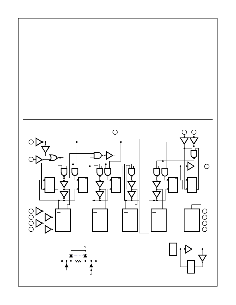
Logic Diagram
CL
CL
2
15
1
9
3
4
5
6
7
R
S
Q
R
S
Q
Q
1
R
S
Q
Q
2
P
4 - 15
R
S
Q
Q
16
R
S
Q
CL
4
LATCHES
CL
CL
4
LATCHES
CL
CL
4
LATCHES
CL
CL
4
LATCHES
CL
3
STATE
OUTPUT
BUFFERS
13
12
11
10
*
*
*
D0
D1
*
D3
*
ALL INPUTS PROTECTED BY
COS/MOS PROTECTION
NETWORK
POS 1
POS 2
POS 3
POS 16
MASTER
RESET
SHIFT
IN
D2
DATA IN READY
(DIR)
SHIFT
OUT
3 - STATE
CONTROL
(OUTPUT
ENABLE)
DATA
READY
(DOR)
Q0
Q1
Q2
Q3
*
*
VDD
VSS
p
n
CL
CL
p
n
DETAIL OF LATCHES
14
相關(guān)PDF資料 |
PDF描述 |
|---|---|
| CD40106BC | Hex Schmitt Trigger(六施密特觸發(fā)器) |
| CD40106BMJ | 16-Bit Transparent D-Type Latch With 3-State Outputs 48-SSOP -40 to 85 |
| CD40106 | CMOS HEX SCHMITT TRIGGERS |
| CD40106BMN | 16-Bit Transparent D-Type Latch With 3-State Outputs 48-SSOP -40 to 85 |
| CD40106 | Hex Schmitt Trigger |
相關(guān)代理商/技術(shù)參數(shù) |
參數(shù)描述 |
|---|---|
| CD40106 | 制造商:INTERSIL 制造商全稱:Intersil Corporation 功能描述:CMOS Hex Schmitt Triggers |
| CD40106_12 | 制造商:UTC-IC 制造商全稱:UTC-IC 功能描述:HEX SCHMITT TRIGGERS |
| CD40106B | 制造商:TI 制造商全稱:Texas Instruments 功能描述:CMOS HEX SCHMITT TRIGGERS |
| CD40106BC | 制造商:FAIRCHILD 制造商全稱:Fairchild Semiconductor 功能描述:Hex Schmitt Trigger |
| CD40106BC_03 | 制造商:FAIRCHILD 制造商全稱:Fairchild Semiconductor 功能描述:Hex Schmitt Trigger |
發(fā)布緊急采購,3分鐘左右您將得到回復(fù)。