- 您現(xiàn)在的位置:買賣IC網(wǎng) > PDF目錄366551 > AM79C976KIW (ADVANCED MICRO DEVICES INC) PCnet-PRO⑩ 10/100 Mbps PCI Ethernet Controller PDF資料下載
參數(shù)資料
| 型號: | AM79C976KIW |
| 廠商: | ADVANCED MICRO DEVICES INC |
| 元件分類: | 微控制器/微處理器 |
| 英文描述: | PCnet-PRO⑩ 10/100 Mbps PCI Ethernet Controller |
| 中文描述: | 1 CHANNEL(S), 100M bps, LOCAL AREA NETWORK CONTROLLER, PQFP208 |
| 封裝: | PLASTIC, QFP-208 |
| 文件頁數(shù): | 62/309頁 |
| 文件大小: | 2070K |
| 代理商: | AM79C976KIW |
第1頁第2頁第3頁第4頁第5頁第6頁第7頁第8頁第9頁第10頁第11頁第12頁第13頁第14頁第15頁第16頁第17頁第18頁第19頁第20頁第21頁第22頁第23頁第24頁第25頁第26頁第27頁第28頁第29頁第30頁第31頁第32頁第33頁第34頁第35頁第36頁第37頁第38頁第39頁第40頁第41頁第42頁第43頁第44頁第45頁第46頁第47頁第48頁第49頁第50頁第51頁第52頁第53頁第54頁第55頁第56頁第57頁第58頁第59頁第60頁第61頁當(dāng)前第62頁第63頁第64頁第65頁第66頁第67頁第68頁第69頁第70頁第71頁第72頁第73頁第74頁第75頁第76頁第77頁第78頁第79頁第80頁第81頁第82頁第83頁第84頁第85頁第86頁第87頁第88頁第89頁第90頁第91頁第92頁第93頁第94頁第95頁第96頁第97頁第98頁第99頁第100頁第101頁第102頁第103頁第104頁第105頁第106頁第107頁第108頁第109頁第110頁第111頁第112頁第113頁第114頁第115頁第116頁第117頁第118頁第119頁第120頁第121頁第122頁第123頁第124頁第125頁第126頁第127頁第128頁第129頁第130頁第131頁第132頁第133頁第134頁第135頁第136頁第137頁第138頁第139頁第140頁第141頁第142頁第143頁第144頁第145頁第146頁第147頁第148頁第149頁第150頁第151頁第152頁第153頁第154頁第155頁第156頁第157頁第158頁第159頁第160頁第161頁第162頁第163頁第164頁第165頁第166頁第167頁第168頁第169頁第170頁第171頁第172頁第173頁第174頁第175頁第176頁第177頁第178頁第179頁第180頁第181頁第182頁第183頁第184頁第185頁第186頁第187頁第188頁第189頁第190頁第191頁第192頁第193頁第194頁第195頁第196頁第197頁第198頁第199頁第200頁第201頁第202頁第203頁第204頁第205頁第206頁第207頁第208頁第209頁第210頁第211頁第212頁第213頁第214頁第215頁第216頁第217頁第218頁第219頁第220頁第221頁第222頁第223頁第224頁第225頁第226頁第227頁第228頁第229頁第230頁第231頁第232頁第233頁第234頁第235頁第236頁第237頁第238頁第239頁第240頁第241頁第242頁第243頁第244頁第245頁第246頁第247頁第248頁第249頁第250頁第251頁第252頁第253頁第254頁第255頁第256頁第257頁第258頁第259頁第260頁第261頁第262頁第263頁第264頁第265頁第266頁第267頁第268頁第269頁第270頁第271頁第272頁第273頁第274頁第275頁第276頁第277頁第278頁第279頁第280頁第281頁第282頁第283頁第284頁第285頁第286頁第287頁第288頁第289頁第290頁第291頁第292頁第293頁第294頁第295頁第296頁第297頁第298頁第299頁第300頁第301頁第302頁第303頁第304頁第305頁第306頁第307頁第308頁第309頁
62
Am79C976
8/01/00
P R E L I M I N A R Y
I
I
To permit the queuing and de-queuing of message
buffers, ownership of each buffer is allocated to either
the Am79C976 controller or the host. The OWN bit
within the descriptor status information, either TMD or
RMD, is used for this purpose.
Setting the OWN to 1 signifies that the Am79C976 con-
troller currently has ownership of this ring descriptor
and its associated buffer. Only the owner is permitted
to relinquish ownership or to write to any field in the de-
scriptor entry. A device that is not the current owner of
a descriptor entry cannot assume ownership or change
any field in the entry. A device may, however, read from
a descriptor that it does not currently own. Software
should always read descriptor entries in sequential or-
der. When software finds that the current descriptor is
owned by the Am79C976 controller, then the software
must not read ahead to the next descriptor. The soft-
ware should wait at a descriptor it does not own until
the Am79C976 controller sets OWN to 0 to release
ownership to the software. (When LAPPEN (CSR3, bit
5) is set to 1, this rule is modified. See the LAPPEN de-
scription.
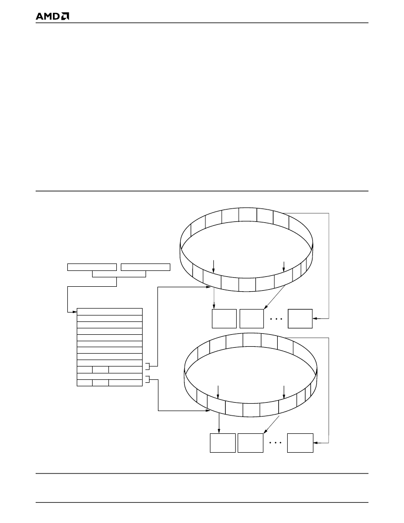
At initialization, the base address of the receive de-
scriptor ring is written to CSR24 (lower 16 bits) and
CSR25 (upper 16 bits), and the base address of the
transmit descriptor ring is written to CSR30 and
CSR31.
Figure 28 illustrates the relationship between the initial-
ization base address, the initialization block, the re-
ceive and transmit descriptor ring base addresses, the
receive and transmit descriptors, and the receive and
transmit data buffers, when SSIZE32 is cleared to 0.
1,-8#
Initialization
Block
MOD
PADR[15:0]
PADR[31:16]
PADR[47:32]
LADRF[15:0]
LADRF[31:16]
LADRF[47:32]
LADRF[63:48]
RDRA[15:0]
RES
IADR[15:0]
IADR[31:16]
CSR1
CSR2
TDRA[15:0]
RES
RLE
RDRA[23:16]
TLE
TDRA[23:16]
Rcv
Buffers
RMDO
RMD1 RMD2
RMD3
Rcv Descriptor
Ring
N
N
N
N
1st
desc.
2nd
desc.
RMD0
Xmt
Buffers
TMD0
TMD1
TMD2
TMD3
Xmt Descriptor
Ring
M
M
M
M
1st
desc.
2nd
desc.
TMD0
Data
Buffer
N
Data
Buffer
1
Data
Buffer
2
Data
Buffer
M
Data
Buffer
1
Data
Buffer
2
相關(guān)PDF資料 |
PDF描述 |
|---|---|
| AM79C976KCW | PCnet-PRO⑩ 10/100 Mbps PCI Ethernet Controller |
| AM79C978AKCW | Single-Chip 1/10 Mbps PCI Home Networking Controller |
| AM79C978AVCW | Single-Chip 1/10 Mbps PCI Home Networking Controller |
| AM79C978 | Single-Chip 1/10 Mbps PCI Home Networking Controller |
| AM79C981 | Integrated Multiport Repeater Plus⑩ (IMR+⑩) |
相關(guān)代理商/技術(shù)參數(shù) |
參數(shù)描述 |
|---|---|
| AM79C978 | 制造商:AMD 制造商全稱:Advanced Micro Devices 功能描述:Single-Chip 1/10 Mbps PCI Home Networking Controller |
| AM79C978A | 制造商:AMD 制造商全稱:Advanced Micro Devices 功能描述:Single-Chip 1/10 Mbps PCI Home Networking Controller |
| AM79C978AKC\\W | 制造商:Advanced Micro Devices 功能描述: |
| AM79C978AKC\W | 制造商:Advanced Micro Devices 功能描述: |
發(fā)布緊急采購,3分鐘左右您將得到回復(fù)。