- 您現(xiàn)在的位置:買賣IC網(wǎng) > PDF目錄375230 > AD1843JS (ANALOG DEVICES INC) CAP 3300PF 100V CERAMIC DISC Y5P PDF資料下載
參數(shù)資料
| 型號: | AD1843JS |
| 廠商: | ANALOG DEVICES INC |
| 元件分類: | 消費家電 |
| 英文描述: | CAP 3300PF 100V CERAMIC DISC Y5P |
| 中文描述: | SPECIALTY CONSUMER CIRCUIT, PQFP80 |
| 封裝: | PLASTIC, QFP-80 |
| 文件頁數(shù): | 42/64頁 |
| 文件大?。?/td> | 848K |
| 代理商: | AD1843JS |
第1頁第2頁第3頁第4頁第5頁第6頁第7頁第8頁第9頁第10頁第11頁第12頁第13頁第14頁第15頁第16頁第17頁第18頁第19頁第20頁第21頁第22頁第23頁第24頁第25頁第26頁第27頁第28頁第29頁第30頁第31頁第32頁第33頁第34頁第35頁第36頁第37頁第38頁第39頁第40頁第41頁當前第42頁第43頁第44頁第45頁第46頁第47頁第48頁第49頁第50頁第51頁第52頁第53頁第54頁第55頁第56頁第57頁第58頁第59頁第60頁第61頁第62頁第63頁第64頁
REV. 0
–42–
AD1843
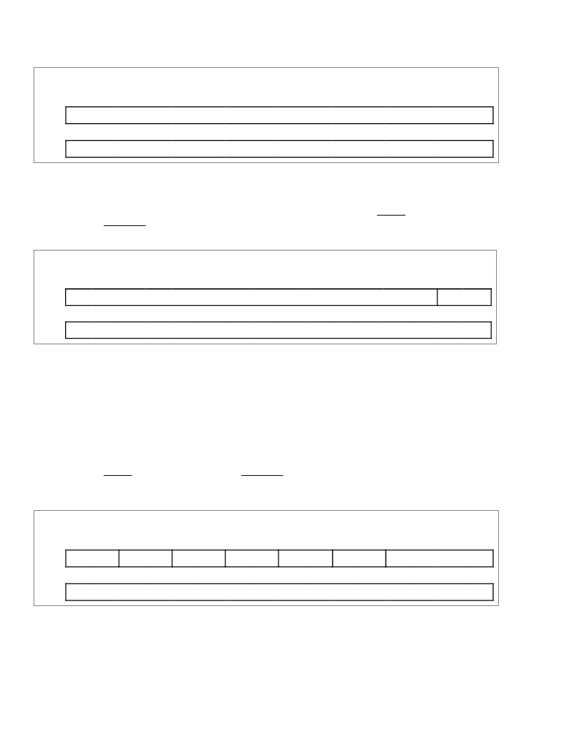
Address 20
Clock Generator 2 Control—Sample Rate
Data 15
Data 14
Data 13
Data 12
Data 11
Data 10
Data 9
Data 8
C2C15
C2C14
C2C13
C2C12
C2C11
C2C10
C2C9
C2C8
Data 7
Data 6
Data 5
Data 4
Data 3
Data 2
Data 1
Data 0
C2C7
C2C6
C2C5
C2C4
C2C3
C2C2
C2C1
C2C0
C2C15:0
Clock Generator 2 Conversion (Sample) Rate Select. Defines the conversion rate produced by Clock Generator 2 when
not referenced to the SYNC2 pin (Control Register Address 19 Bit 15 [C2REF]). One LSB represents exactly one Hertz,
assuming a 24.576MHz clock input on the XTALI pin. Usable range is 4 kHz (0x0FA0) to 54 kHz (0xD2F0).
Initial default state after reset: 1011 1011 1000 0000 (BB80 hex), which is 48 kHz, assuming a 24.576 MHz clock in-
put on the XTALI pin. Cleared to default and cannot be written to when: the
RESET
pin is asserted LO; or when
the
PWRDWN
pin is asserted LO.
Address 21
Clock Generator 2 Control—Sample Phase Shift
Data 15
Data 14
Data 13
Data 12
Data 11
Data 10
Data 9
Data 8
res
res
res
res
res
res
res
C2PD
Data 7
Data 6
Data 5
Data 4
Data 3
Data 2
Data 1
Data 0
C2P7
C2P6
C2P5
C2P4
C2P3
C2P2
C2P1
C2P0
C2PD
Clock Generator 2 Phase Shift Direction. This bit controls the direction of sample clock phase shift.
0
= Phase Advance
1 = Phase Retard
Clock Generator 2 Phase Shift Magnitude. These bits control the magnitude of sample clock phase shift. One LSB repre-
sents exactly 0.12 degrees. LSBs are processed and decremented at a rate of 3.072 MHz (assuming a 24.576 MHz clock
input on the XTALI pin). When this register is read, it indicates any phase advance/retard remaining to be processed as of
the beginning of slot 0 if bus master, or when TSI was received if bus slave. This register may be overwritten even if all pre-
viously programmed phase advance/retard has not been processed. When written, the contents of this register (just prior to
the write) are transmitted during slot 1 of the following frame (as with all Control Register writes).
Reserved for future expansion. To ensure future compatibility, write “0” to all reserved bits.
Initial default state after reset: 0000 0000 0000 0000 (0000 hex). Cleared to default and cannot be written to when:
the
RESET
pin is asserted LO; when the
PWRDWN
pin is asserted LO; or when the G2EN bit in Control Register
Address 28 is reset to “0” (clock generator 2 disabled).
C2P7:0
res
Address 22
Clock Generator 3 Control—Mode
Data 15
Data 14
Data 13
Data 12
Data 11
Data 10
Data 9
Data 8
C3REF
C3VID
C3PLLG
C3P200
C3X8/7
C3C128
res
res
Data 7
Data 6
Data 5
Data 4
Data 3
Data 2
Data 1
Data 0
C3M7
C3M6
C3M5
C3M4
C3M3
C3M2
C3M1
C3M0
C3REF
Clock Generator 3 Reference Select. Selects the fundamental clock reference used by Clock Generator 3 to synthe-
size its “Conversion” (sample) and “Bit” clock rates.
0
= Clocks are referenced to the input on pin XTALI (crystal or master clock input).
Sample clock frequency is defined by Control Register Address 23 and Bit C3X8/7.
Sample clock phase may be shifted by Control Register Address 24.
Bit clock frequency is defined by bits C3M7:0 and C3P200.
Bit C3VID is ignored.
相關(guān)PDF資料 |
PDF描述 |
|---|---|
| AD1843JST | Serial-Port 16-Bit SoundComm Codec |
| AD1846JP | Low Cost Parallel-Port 16-Bit SoundPort Stereo Codec |
| AD1849KP | Serial-Port 16-Bit SoundPort Stereo Codec |
| AD1851 | 16-Bit, 16×Fs PCM Audio DACs(16位,單片PCM音頻D/A轉(zhuǎn)換器) |
| AD1892JR | Integrated Digital Receiver/Rate Converter |
相關(guān)代理商/技術(shù)參數(shù) |
參數(shù)描述 |
|---|---|
| AD1843JST | 制造商:AD 制造商全稱:Analog Devices 功能描述:Serial-Port 16-Bit SoundComm Codec |
| AD1845 | 制造商:AD 制造商全稱:Analog Devices 功能描述:Parallel-Port 16-Bit SoundPort Stereo Codec |
| AD1845JP | 制造商:Analog Devices 功能描述:Audio Codec 2ADC / 2DAC 16-Bit 68-Pin PLCC 制造商:Rochester Electronics LLC 功能描述:16 BIT AUDIO CODEC - Bulk 制造商:Analog Devices 功能描述:IC CODEC 16-BIT AUDIO |
| AD1845JP-REEL | 制造商:Analog Devices 功能描述:Audio Codec 2ADC / 2DAC 16-Bit 68-Pin PLCC T/R |
| AD1845JPZ | 制造商:Analog Devices 功能描述:Audio Codec 2ADC / 2DAC 16-Bit 68-Pin PLCC |
發(fā)布緊急采購,3分鐘左右您將得到回復。