- 您現(xiàn)在的位置:買賣IC網(wǎng) > PDF目錄36339 > 935273916557 (NXP SEMICONDUCTORS) COLOR SIGNAL DECODER, PBGA156 PDF資料下載
參數(shù)資料
| 型號: | 935273916557 |
| 廠商: | NXP SEMICONDUCTORS |
| 元件分類: | 顏色信號轉(zhuǎn)換 |
| 英文描述: | COLOR SIGNAL DECODER, PBGA156 |
| 封裝: | 15 X 15 MM, 1.15 MM HEIGHT, PLASTIC, MS-034, SOT-472-1, BGA-156 |
| 文件頁數(shù): | 174/178頁 |
| 文件大?。?/td> | 988K |
| 代理商: | 935273916557 |
第1頁第2頁第3頁第4頁第5頁第6頁第7頁第8頁第9頁第10頁第11頁第12頁第13頁第14頁第15頁第16頁第17頁第18頁第19頁第20頁第21頁第22頁第23頁第24頁第25頁第26頁第27頁第28頁第29頁第30頁第31頁第32頁第33頁第34頁第35頁第36頁第37頁第38頁第39頁第40頁第41頁第42頁第43頁第44頁第45頁第46頁第47頁第48頁第49頁第50頁第51頁第52頁第53頁第54頁第55頁第56頁第57頁第58頁第59頁第60頁第61頁第62頁第63頁第64頁第65頁第66頁第67頁第68頁第69頁第70頁第71頁第72頁第73頁第74頁第75頁第76頁第77頁第78頁第79頁第80頁第81頁第82頁第83頁第84頁第85頁第86頁第87頁第88頁第89頁第90頁第91頁第92頁第93頁第94頁第95頁第96頁第97頁第98頁第99頁第100頁第101頁第102頁第103頁第104頁第105頁第106頁第107頁第108頁第109頁第110頁第111頁第112頁第113頁第114頁第115頁第116頁第117頁第118頁第119頁第120頁第121頁第122頁第123頁第124頁第125頁第126頁第127頁第128頁第129頁第130頁第131頁第132頁第133頁第134頁第135頁第136頁第137頁第138頁第139頁第140頁第141頁第142頁第143頁第144頁第145頁第146頁第147頁第148頁第149頁第150頁第151頁第152頁第153頁第154頁第155頁第156頁第157頁第158頁第159頁第160頁第161頁第162頁第163頁第164頁第165頁第166頁第167頁第168頁第169頁第170頁第171頁第172頁第173頁當(dāng)前第174頁第175頁第176頁第177頁第178頁
2004
Jul
22
95
Philips
Semiconductors
Product
speci
cation
Multistandard
video
decoder
with
adaptiv
e
comb
lter
and
component
video
input
SAA7118
2004
Jul
22
95
Philips
Semiconductors
Product
speci
cation
Multistandard
video
decoder
with
adaptiv
e
comb
lter
and
component
video
input
SAA7118
This text is here in white to force landscape pages to be rotated correctly when browsing through the pdf in the Acrobat reader.This text is here in
_white to force landscape pages to be rotated correctly when browsing through the pdf in the Acrobat reader.This text is here inThis text is here in
white to force landscape pages to be rotated correctly when browsing through the pdf in the Acrobat reader. white to force landscape pages to be ...
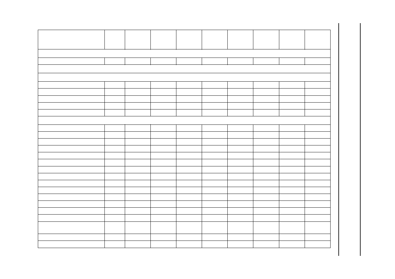
Table 38 I2C-bus receiver/transmitter overview
REGISTER FUNCTION
SUB
ADDR.
(HEX)
D7
D6
D5
D4
D3
D2
D1
D0
Chip version: register 00H
Chip version (read only)
00
ID7
ID6
ID5
ID4
Video decoder: registers 01H to 1FH
FRONT-END PART: REGISTERS 01H TO 05H
Increment delay
01
WPOFF
GUDL1
GUDL0
IDEL3
IDEL2
IDEL1
IDEL0
Analog input control 1
02
FUSE1
FUSE0
MODE5
MODE4
MODE3
MODE2
MODE1
MODE0
Analog input control 2
03
HLNRS
VBSL
CPOFF
HOLDG
GAFIX
GAI28
GAI18
Analog input control 3
04
GAI17
GAI16
GAI15
GAI14
GAI13
GAI12
GAI11
GAI10
Analog input control 4
05
GAI27
GAI26
GAI25
GAI24
GAI23
GAI22
GAI21
GAI20
DECODER PART: REGISTERS 06H TO 1FH
Horizontal sync start
06
HSB7
HSB6
HSB5
HSB4
HSB3
HSB2
HSB1
HSB0
Horizontal sync stop
07
HSS7
HSS6
HSS5
HSS4
HSS3
HSS2
HSS1
HSS0
Sync control
08
AUFD
FSEL
FOET
HTC1
HTC0
HPLL
VNOI1
VNOI0
Luminance control
09
BYPS
YCOMB
LDEL
LUBW
LUFI3
LUFI2
LUFI1
LUFI0
Luminance brightness control
0A
DBRI7
DBRI6
DBRI5
DBRI4
DBRI3
DBRI2
DBRI1
DBRI0
Luminance contrast control
0B
DCON7
DCON6
DCON5
DCON4
DCON3
DCON2
DCON1
DCON0
Chrominance saturation control
0C
DSAT7
DSAT6
DSAT5
DSAT4
DSAT3
DSAT2
DSAT1
DSAT0
Chrominance hue control
0D
HUEC7
HUEC6
HUEC5
HUEC4
HUEC3
HUEC2
HUEC1
HUEC0
Chrominance control 1
0E
CDTO
CSTD2
CSTD1
CSTD0
DCVF
FCTC
AUTO0
CCOMB
Chrominance gain control
0F
ACGC
CGAIN6
CGAIN5
CGAIN4
CGAIN3
CGAIN2
CGAIN1
CGAIN0
Chrominance control 2
10
OFFU1
OFFU0
OFFV1
OFFV0
CHBW
LCBW2
LCBW1
LCBW0
Mode/delay control
11
COLO
RTP1
HDEL1
HDEL0
RTP0
YDEL2
YDEL1
YDEL0
RT signal control
12
RTSE13
RTSE12
RTSE11
RTSE10
RTSE03
RTSE02
RTSE01
RTSE00
RT/X port output control
13
RTCE
XRHS
XRVS1
XRVS0
HLSEL
OFTS2
OFTS1
OFTS0
Analog/ADC/compatibility
control
14
CM99
UPTCV
AOSL1
AOSL0
XTOUTE
AUTO1
APCK1
APCK0
VGATE start, FID change
15
VSTA7
VSTA6
VSTA5
VSTA4
VSTA3
VSTA2
VSTA1
VSTA0
VGATE stop
16
VSTO7
VSTO6
VSTO5
VSTO4
VSTO3
VSTO2
VSTO1
VSTO0
相關(guān)PDF資料 |
PDF描述 |
|---|---|
| 935268460118 | 1-CHANNEL, SGL POLE SGL THROW SWITCH, PDSO5 |
| 935268459115 | 1-CHANNEL, SGL POLE SGL THROW SWITCH, PDSO5 |
| 935268459118 | 1-CHANNEL, SGL POLE SGL THROW SWITCH, PDSO5 |
| 935268459125 | 1-CHANNEL, SGL POLE SGL THROW SWITCH, PDSO5 |
| 935268459165 | 1-CHANNEL, SGL POLE SGL THROW SWITCH, PDSO5 |
相關(guān)代理商/技術(shù)參數(shù) |
參數(shù)描述 |
|---|---|
| 935275527134 | 制造商:NXP Semiconductors 功能描述:IC BUS SWITCH OCTAL QUAD 20TSSOP |
| 935277864112 | 制造商:NXP Semiconductors 功能描述:IC CPU |
| 935278818112 | 制造商:NXP Semiconductors 功能描述:LCD DRVR 20DIGIT 2.5V/3.3V/5V 56-Pin VSO Tube |
| 935280517132 | 制造商:NXP Semiconductors 功能描述:IC TRANSLATING BUFFER 6XSON |
| 935281751112 | 制造商:NXP Semiconductors 功能描述:IC BUFFER/DVR 16BIT 3ST 48TSSOP |
發(fā)布緊急采購,3分鐘左右您將得到回復(fù)。