- 您現(xiàn)在的位置:買賣IC網(wǎng) > PDF目錄36339 > 935273916557 (NXP SEMICONDUCTORS) COLOR SIGNAL DECODER, PBGA156 PDF資料下載
參數(shù)資料
| 型號: | 935273916557 |
| 廠商: | NXP SEMICONDUCTORS |
| 元件分類: | 顏色信號轉(zhuǎn)換 |
| 英文描述: | COLOR SIGNAL DECODER, PBGA156 |
| 封裝: | 15 X 15 MM, 1.15 MM HEIGHT, PLASTIC, MS-034, SOT-472-1, BGA-156 |
| 文件頁數(shù): | 136/178頁 |
| 文件大小: | 988K |
| 代理商: | 935273916557 |
第1頁第2頁第3頁第4頁第5頁第6頁第7頁第8頁第9頁第10頁第11頁第12頁第13頁第14頁第15頁第16頁第17頁第18頁第19頁第20頁第21頁第22頁第23頁第24頁第25頁第26頁第27頁第28頁第29頁第30頁第31頁第32頁第33頁第34頁第35頁第36頁第37頁第38頁第39頁第40頁第41頁第42頁第43頁第44頁第45頁第46頁第47頁第48頁第49頁第50頁第51頁第52頁第53頁第54頁第55頁第56頁第57頁第58頁第59頁第60頁第61頁第62頁第63頁第64頁第65頁第66頁第67頁第68頁第69頁第70頁第71頁第72頁第73頁第74頁第75頁第76頁第77頁第78頁第79頁第80頁第81頁第82頁第83頁第84頁第85頁第86頁第87頁第88頁第89頁第90頁第91頁第92頁第93頁第94頁第95頁第96頁第97頁第98頁第99頁第100頁第101頁第102頁第103頁第104頁第105頁第106頁第107頁第108頁第109頁第110頁第111頁第112頁第113頁第114頁第115頁第116頁第117頁第118頁第119頁第120頁第121頁第122頁第123頁第124頁第125頁第126頁第127頁第128頁第129頁第130頁第131頁第132頁第133頁第134頁第135頁當前第136頁第137頁第138頁第139頁第140頁第141頁第142頁第143頁第144頁第145頁第146頁第147頁第148頁第149頁第150頁第151頁第152頁第153頁第154頁第155頁第156頁第157頁第158頁第159頁第160頁第161頁第162頁第163頁第164頁第165頁第166頁第167頁第168頁第169頁第170頁第171頁第172頁第173頁第174頁第175頁第176頁第177頁第178頁
2004 Jul 22
60
Philips Semiconductors
Product specication
Multistandard video decoder with adaptive
comb lter and component video input
SAA7118
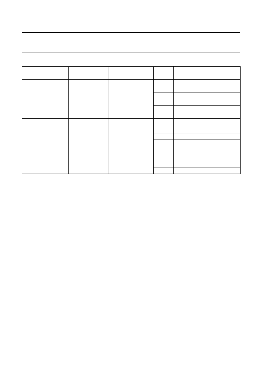
Table 14 Vertical phase offset usage; assignment of the phase offsets
Notes
1. Case 1: OFIDC[90H[6]] = 0; scaler input field ID as output ID; back-end interprets output field ID at logic 0 as upper
output lines.
2. Case 2: OFIDC[90H[6]] = 1; task status bit as output ID; back-end interprets output field ID at logic 0 as upper output
lines.
3. Case 3: OFIDC[90H[6]] = 1; task status bit as output ID; back-end interprets output field ID at logic 1 as upper output
lines.
DETECTED INPUT
FIELD ID
TASK STATUS BIT
VERTICAL PHASE
OFFSET
CASE
EQUATION TO BE USED
0 = upper lines
0
YPY0[7:0] and
YPC0[7:0]
case 1(1) UP-UP (PHO)
case 2(2) UP-UP
case 3(3) UP-LO
0 = upper lines
1
YPY1[7:0] and
YPC1[7:0]
case 1
UP-UP (PHO)
case 2
UP-LO
case 3
UP-UP
1 = lower lines
0
YPY2[7:0] and
YPC2[7:0]
case 1
LO-LO
case 2
LO-UP
case 3
LO-LO
1 = lower lines
1
YPY3[7:0] and
YPC3[7:0]
case 1
LO-LO
case 2
LO-LO
case 3
LO-UP
PHO
YSCY[15:0]
64
-------------------------------
16
–
+
PHO
YSCY[15:0]
64
-------------------------------
16
–
+
8.5
VBI data decoder and capture
(subaddresses 40H to 7FH)
The SAA7118 contains a versatile VBI data decoder.
The implementation and programming model is in
accordance with the VBI data slicer built into the
multimedia video data acquisition circuit SAA5284.
The circuitry recovers the actual clock phase during the
clock run-in period, slices the data bits with the selected
data rate, and groups them into bytes. The result is
buffered into a dedicated VBI data FIFO with a capacity of
2
× 56 bytes (2 × 14 Dwords). The clock frequency, signal
source, field frequency and accepted error count must be
defined in subaddress 40H.
The supported VBI data standards are shown in Table 15.
For lines 2 to 24 of a field, per VBI line, 1 of 16 standards
can be selected (LCR24_[7:0] to LCR2_[7:0] in 57H[7:0] to
41H[7:0]: 23
× 2 × 4 bit programming bits).
The definition for line 24 is valid for the rest of the
corresponding field, normally no text data (video data)
should be selected there (LCR24_[7:0] = FFH) to stop the
activity of the VBI data slicer during active video.
To adjust the slicers processing to the input signal source,
there are offsets in the horizontal and vertical direction
available: parameters HOFF[10:0] 5BH[2:0] 59H[7:0],
VOFF[8:0] 5BH[4] 5AH[7:0] and FOFF[5BH[7]].
Contrary to the scalers counting, the slicers offsets define
the position of the H and V trigger events related to the
processed video field. The trigger events are the falling
edge of HREF and the falling edge of V123 from the
decoder processing part.
The relationship of these programming values to the input
signal and the recommended values are given in
相關(guān)PDF資料 |
PDF描述 |
|---|---|
| 935268460118 | 1-CHANNEL, SGL POLE SGL THROW SWITCH, PDSO5 |
| 935268459115 | 1-CHANNEL, SGL POLE SGL THROW SWITCH, PDSO5 |
| 935268459118 | 1-CHANNEL, SGL POLE SGL THROW SWITCH, PDSO5 |
| 935268459125 | 1-CHANNEL, SGL POLE SGL THROW SWITCH, PDSO5 |
| 935268459165 | 1-CHANNEL, SGL POLE SGL THROW SWITCH, PDSO5 |
相關(guān)代理商/技術(shù)參數(shù) |
參數(shù)描述 |
|---|---|
| 935275527134 | 制造商:NXP Semiconductors 功能描述:IC BUS SWITCH OCTAL QUAD 20TSSOP |
| 935277864112 | 制造商:NXP Semiconductors 功能描述:IC CPU |
| 935278818112 | 制造商:NXP Semiconductors 功能描述:LCD DRVR 20DIGIT 2.5V/3.3V/5V 56-Pin VSO Tube |
| 935280517132 | 制造商:NXP Semiconductors 功能描述:IC TRANSLATING BUFFER 6XSON |
| 935281751112 | 制造商:NXP Semiconductors 功能描述:IC BUFFER/DVR 16BIT 3ST 48TSSOP |
發(fā)布緊急采購,3分鐘左右您將得到回復(fù)。