- 您現(xiàn)在的位置:買賣IC網(wǎng) > PDF目錄156423 > 34C60 (SMSC Corporation) PARALLEL PORT INTERFACE CHIP PERIPHERAL SIDE PDF資料下載
參數(shù)資料
| 型號(hào): | 34C60 |
| 廠商: | SMSC Corporation |
| 英文描述: | PARALLEL PORT INTERFACE CHIP PERIPHERAL SIDE |
| 中文描述: | 并行接口芯片外設(shè)端 |
| 文件頁(yè)數(shù): | 28/58頁(yè) |
| 文件大小: | 350K |
| 代理商: | 34C60 |
第1頁(yè)第2頁(yè)第3頁(yè)第4頁(yè)第5頁(yè)第6頁(yè)第7頁(yè)第8頁(yè)第9頁(yè)第10頁(yè)第11頁(yè)第12頁(yè)第13頁(yè)第14頁(yè)第15頁(yè)第16頁(yè)第17頁(yè)第18頁(yè)第19頁(yè)第20頁(yè)第21頁(yè)第22頁(yè)第23頁(yè)第24頁(yè)第25頁(yè)第26頁(yè)第27頁(yè)當(dāng)前第28頁(yè)第29頁(yè)第30頁(yè)第31頁(yè)第32頁(yè)第33頁(yè)第34頁(yè)第35頁(yè)第36頁(yè)第37頁(yè)第38頁(yè)第39頁(yè)第40頁(yè)第41頁(yè)第42頁(yè)第43頁(yè)第44頁(yè)第45頁(yè)第46頁(yè)第47頁(yè)第48頁(yè)第49頁(yè)第50頁(yè)第51頁(yè)第52頁(yè)第53頁(yè)第54頁(yè)第55頁(yè)第56頁(yè)第57頁(yè)第58頁(yè)
SMSC DS – PPC34C60
Rev. 06/01/2001
ADVANCED INFORMATION
7
OPERATIONAL DESCRIPTION
MAXIMUM GUARANTEED RATINGS*
Operating Temperature Range................................................................................................................................0
oC to +70oC
Storage Temperature Range................................................................................................................................ -55
o to +150oC
Lead Temperature Range (soldering, 10 seconds)..........................................................................................................+325
oC
Positive Voltage on any pin, with respect to Ground...................................................................................................VCC+0.3V
Negative Voltage on any pin, with respect to Ground ......................................................................................................... -0.3V
Maximum VCC........................................................................................................................................................................+7V
*Stresses above those listed above could cause permanent damage to the device. This is a stress rating only and
functional operation of the device at any other condition above those indicated in the operation sections of this specification
is not implied.
Note: When powering this device from laboratory or system power supplies, it is important that the Absolute Maximum
Ratings not be exceeded or device failure can result. Some power supplies exhibit voltage spikes on their outputs when the
AC power is switched on or off. In addition, voltage transients on the AC power line may appear on the DC output. If this
possibility exists, it is suggested that a clamp circuit be used.
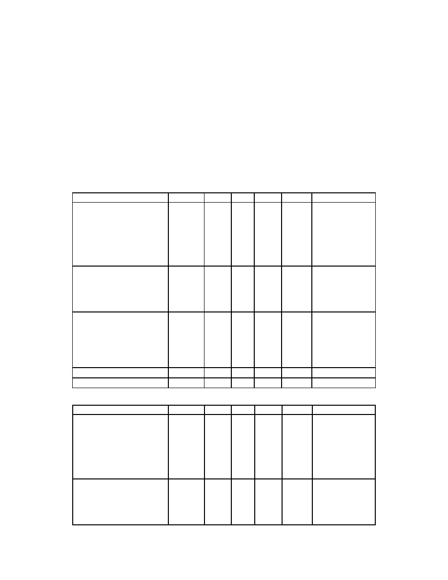
DC ELECTRICAL CHARACTERISTICS (TA = 0
oC - 70oC, VCC = +5.0 V ± 10%)
PARAMETER
SYMBOL
MIN
TYP
MAX
UNITS
COMMENTS
I Type Input Buffer
Low Input Level
High Input Level
Schmitt Trigger Hysteresis
VILIS
VIHIS
VHYS
2.2
250
0.8
V
mV
Schmitt Trigger
ICLK Input Buffer
Low Input Level
High Input Level
VILCK
VIHCK
3.0
0.4
V
Input Leakage
(All I and IS buffers)
Low Input Leakage
High Input Leakage
IIL
IIH
-10
+10
A
VIN = 0
VIN = VCC
Pull Up Current
IOH
75
150
A
VIN = 0
Pull Down Current
IOL
200
A
VIN = 5
PARAMETER
SYMBOL
MIN
TYP
MAX
UNITS
COMMENTS
I/O8 Type Buffer
Low Output Level
High Output Level
Output Leakage
VOL
VOH
IOL
2.4
-10
0.4
+10
V
A
IOL = 8 mA
IOH = -4 mA
VIN = 0 to VCC
I/O16 Type Buffer
Low Output Level
High Output Level
VOL
VOH
2.4
0.4
V
IOL = 16 mA
IOH = -12 mA
相關(guān)PDF資料 |
PDF描述 |
|---|---|
| 34CMDP25B5M1RT | TOGGLE SWITCH, DPDT, MOMENTARY, 0.02A, 20VDC, PANEL MOUNT-THREADED |
| 34CMDP25B3V3RT | TOGGLE SWITCH, DPDT, MOMENTARY, 0.02A, 20VDC, THROUGH HOLE-STRAIGHT |
| 34CMDP43B4V2QT | TOGGLE SWITCH, DPDT, MOMENTARY, 3A, 28VDC, THROUGH HOLE-STRAIGHT |
| 34CMDP13B1M6RT | TOGGLE SWITCH, DPDT, LATCHED, 0.02A, 20VDC, THROUGH HOLE-RIGHT ANGLE |
| 34CMDP12B3M6QT | TOGGLE SWITCH, DPDT, LATCHED, 3A, 28VDC, THROUGH HOLE-RIGHT ANGLE |
相關(guān)代理商/技術(shù)參數(shù) |
參數(shù)描述 |
|---|---|
| 34C7561 | 制造商:未知廠家 制造商全稱:未知廠家 功能描述:DESIGN CENTER |
| 34C7563 | 制造商:未知廠家 制造商全稱:未知廠家 功能描述:PLCC BREAKOUT ADAPTER BOARD |
| 34C7564 | 制造商:未知廠家 制造商全稱:未知廠家 功能描述:PLCC 68 BREAKOUT ADAPTER BRD |
| 34C7565 | 制造商:未知廠家 制造商全稱:未知廠家 功能描述:PLCC 84 BREAKOUT ADAPTER BRD |
| 34C7566 | 制造商:未知廠家 制造商全稱:未知廠家 功能描述:QFP 208 BREAKOUT ADAPTER BRD |
發(fā)布緊急采購(gòu),3分鐘左右您將得到回復(fù)。