- 您現(xiàn)在的位置:買賣IC網(wǎng) > PDF目錄1973 > XC3SD1800A-4CSG484LI (Xilinx Inc)IC FPGA SPARTAN 3 DSP 484CSGBGA PDF資料下載
參數(shù)資料
| 型號: | XC3SD1800A-4CSG484LI |
| 廠商: | Xilinx Inc |
| 文件頁數(shù): | 16/101頁 |
| 文件大?。?/td> | 0K |
| 描述: | IC FPGA SPARTAN 3 DSP 484CSGBGA |
| 標(biāo)準(zhǔn)包裝: | 84 |
| 系列: | Spartan®-3A DSP |
| LAB/CLB數(shù): | 4160 |
| 邏輯元件/單元數(shù): | 37440 |
| RAM 位總計: | 1548288 |
| 輸入/輸出數(shù): | 309 |
| 門數(shù): | 1800000 |
| 電源電壓: | 1.14 V ~ 1.26 V |
| 安裝類型: | 表面貼裝 |
| 工作溫度: | -40°C ~ 100°C |
| 封裝/外殼: | 484-FBGA,CSPBGA |
| 供應(yīng)商設(shè)備封裝: | 484-CSPBGA |
第1頁第2頁第3頁第4頁第5頁第6頁第7頁第8頁第9頁第10頁第11頁第12頁第13頁第14頁第15頁當(dāng)前第16頁第17頁第18頁第19頁第20頁第21頁第22頁第23頁第24頁第25頁第26頁第27頁第28頁第29頁第30頁第31頁第32頁第33頁第34頁第35頁第36頁第37頁第38頁第39頁第40頁第41頁第42頁第43頁第44頁第45頁第46頁第47頁第48頁第49頁第50頁第51頁第52頁第53頁第54頁第55頁第56頁第57頁第58頁第59頁第60頁第61頁第62頁第63頁第64頁第65頁第66頁第67頁第68頁第69頁第70頁第71頁第72頁第73頁第74頁第75頁第76頁第77頁第78頁第79頁第80頁第81頁第82頁第83頁第84頁第85頁第86頁第87頁第88頁第89頁第90頁第91頁第92頁第93頁第94頁第95頁第96頁第97頁第98頁第99頁第100頁第101頁
Spartan-3A DSP FPGA Family: DC and Switching Characteristics
DS610 (v3.0) October 4, 2010
Product Specification
21
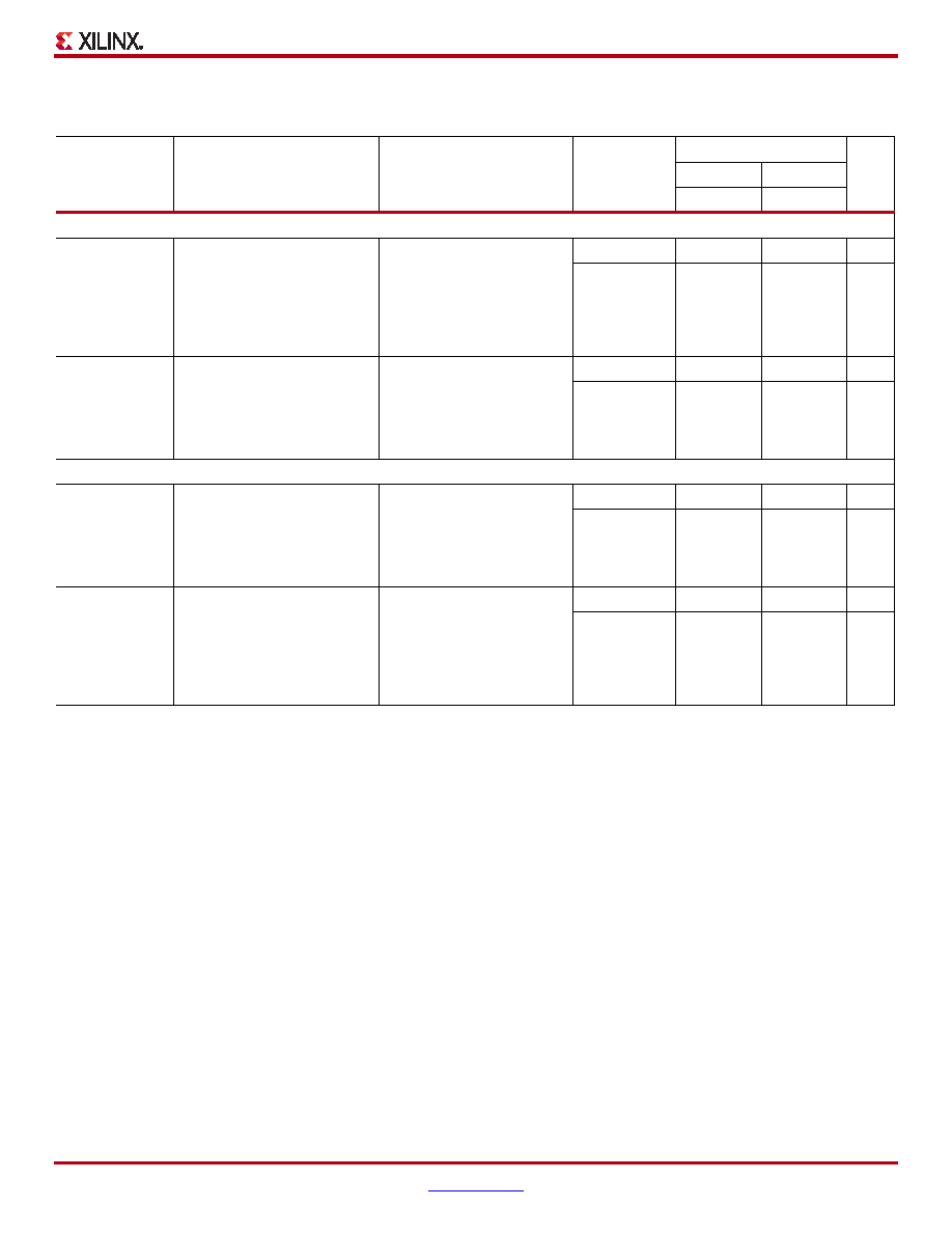
Pin-to-Pin Setup and Hold Times
Table 18: Pin-to-Pin Setup and Hold Times for the IOB Input Path (System Synchronous)
Symbol
Description
Conditions
Device
Speed Grade
Units
-5
-4
Max
Setup Times
TPSDCM
When writing to the Input
Flip-Flop (IFF), the time from
the setup of data at the Input pin
to the active transition at a
Global Clock pin. The DCM is in
use. No Input Delay is
programmed.
LVCMOS25(2),
IFD_DELAY_VALUE = 0,
with DCM(4)
XC3SD1800A
2.65
3.11
ns
XC3SD3400A
2.25
2.49
ns
TPSFD
When writing to IFF, the time
from the setup of data at the
Input pin to an active transition
at the Global Clock pin. The
DCM is not in use. The Input
Delay is programmed.
LVCMOS25(2),
IFD_DELAY_VALUE = 6,
without DCM
XC3SD1800A
2.98
3.39
ns
XC3SD3400A
2.78
3.08
ns
Hold Times
TPHDCM
When writing to IFF, the time
from the active transition at the
Global Clock pin to the point
when data must be held at the
Input pin. The DCM is in use.
No Input Delay is programmed.
LVCMOS25(3),
IFD_DELAY_VALUE = 0,
with DCM(4)
XC3SD1800A
–0.38
ns
XC3SD3400A
–0.26
ns
TPHFD
When writing to IFF, the time
from the active transition at the
Global Clock pin to the point
when data must be held at the
Input pin. The DCM is not in
use. The Input Delay is
programmed.
LVCMOS25(3),
IFD_DELAY_VALUE = 6,
without DCM
XC3SD1800A
–0.71
ns
XC3SD3400A
–0.65
ns
Notes:
1.
The numbers in this table are tested using the methodology presented in Table 26 and are based on the operating conditions set forth in
2.
This setup time requires adjustment whenever a signal standard other than LVCMOS25 is assigned to the Global Clock Input or the data
Input. If this is true of the Global Clock Input, subtract the appropriate adjustment from Table 22. If this is true of the data Input, add the
appropriate Input adjustment from the same table.
3.
This hold time requires adjustment whenever a signal standard other than LVCMOS25 is assigned to the Global Clock Input or the data
Input. If this is true of the Global Clock Input, add the appropriate Input adjustment from Table 22. If this is true of the data Input, subtract the
appropriate Input adjustment from the same table. When the hold time is negative, it is possible to change the data before the clock’s active
edge.
4.
DCM output jitter is included in all measurements.
相關(guān)PDF資料 |
PDF描述 |
|---|---|
| XC3SD3400A-4FGG676I | SPARTAN-3ADSP FPGA 3400K 676FBGA |
| XC4036XLA-09HQ240C | IC FPGA C 2.5V 288 I/O 240HQFP |
| XC4062XL-09HQ240C | IC FPGA C-TEMP 3.3V 240-HQFP |
| XC4085XL-3BG560I | IC FPGA I-TEMP 3.3V 3SPD 560MBGA |
| XC4VLX100-10FFG1513C | IC FPGA VIRTEX-4 100K 1513-FBGA |
相關(guān)代理商/技術(shù)參數(shù) |
參數(shù)描述 |
|---|---|
| XC3SD1800A-4FG676C | 制造商:Xilinx 功能描述:FPGA SPARTAN-3A 1.8M GATES 37440 CELLS 667MHZ 1.2V 676FBGA - Trays 制造商:Xilinx 功能描述:IC FPGA 519 I/O 676FBGA 制造商:Xilinx 功能描述:SPARTAN-3ADSP FPGA 1800K 676FBGA |
| XC3SD1800A-4FG676I | 功能描述:SPARTAN-3ADSP FPGA 1800K 676FBGA RoHS:否 類別:集成電路 (IC) >> 嵌入式 - FPGA(現(xiàn)場可編程門陣列) 系列:Spartan®-3A DSP 標(biāo)準(zhǔn)包裝:40 系列:Spartan® 6 LX LAB/CLB數(shù):3411 邏輯元件/單元數(shù):43661 RAM 位總計:2138112 輸入/輸出數(shù):358 門數(shù):- 電源電壓:1.14 V ~ 1.26 V 安裝類型:表面貼裝 工作溫度:-40°C ~ 100°C 封裝/外殼:676-BGA 供應(yīng)商設(shè)備封裝:676-FBGA(27x27) |
| XC3SD1800A-4FGG676C | 功能描述:SPARTAN-3ADSP FPGA 1800K 676FBGA RoHS:是 類別:集成電路 (IC) >> 嵌入式 - FPGA(現(xiàn)場可編程門陣列) 系列:Spartan®-3A DSP 標(biāo)準(zhǔn)包裝:24 系列:ECP2 LAB/CLB數(shù):1500 邏輯元件/單元數(shù):12000 RAM 位總計:226304 輸入/輸出數(shù):131 門數(shù):- 電源電壓:1.14 V ~ 1.26 V 安裝類型:表面貼裝 工作溫度:0°C ~ 85°C 封裝/外殼:208-BFQFP 供應(yīng)商設(shè)備封裝:208-PQFP(28x28) |
| XC3SD1800A-4FGG676CES | 制造商:Xilinx 功能描述: |
| XC3SD1800A-4FGG676I | 功能描述:SPARTAN-3ADSP FPGA 1800K 676FBGA RoHS:是 類別:集成電路 (IC) >> 嵌入式 - FPGA(現(xiàn)場可編程門陣列) 系列:Spartan®-3A DSP 標(biāo)準(zhǔn)包裝:40 系列:Spartan® 6 LX LAB/CLB數(shù):3411 邏輯元件/單元數(shù):43661 RAM 位總計:2138112 輸入/輸出數(shù):358 門數(shù):- 電源電壓:1.14 V ~ 1.26 V 安裝類型:表面貼裝 工作溫度:-40°C ~ 100°C 封裝/外殼:676-BGA 供應(yīng)商設(shè)備封裝:676-FBGA(27x27) |
發(fā)布緊急采購,3分鐘左右您將得到回復(fù)。