- 您現(xiàn)在的位置:買賣IC網 > PDF目錄383983 > UPD75236 (NEC Corp.) 4-BIT SINGLE-CHIP MICROCOMPUTER PDF資料下載
參數資料
| 型號: | UPD75236 |
| 廠商: | NEC Corp. |
| 英文描述: | 4-BIT SINGLE-CHIP MICROCOMPUTER |
| 中文描述: | 4位單片機 |
| 文件頁數: | 89/190頁 |
| 文件大小: | 1220K |
| 代理商: | UPD75236 |
第1頁第2頁第3頁第4頁第5頁第6頁第7頁第8頁第9頁第10頁第11頁第12頁第13頁第14頁第15頁第16頁第17頁第18頁第19頁第20頁第21頁第22頁第23頁第24頁第25頁第26頁第27頁第28頁第29頁第30頁第31頁第32頁第33頁第34頁第35頁第36頁第37頁第38頁第39頁第40頁第41頁第42頁第43頁第44頁第45頁第46頁第47頁第48頁第49頁第50頁第51頁第52頁第53頁第54頁第55頁第56頁第57頁第58頁第59頁第60頁第61頁第62頁第63頁第64頁第65頁第66頁第67頁第68頁第69頁第70頁第71頁第72頁第73頁第74頁第75頁第76頁第77頁第78頁第79頁第80頁第81頁第82頁第83頁第84頁第85頁第86頁第87頁第88頁當前第89頁第90頁第91頁第92頁第93頁第94頁第95頁第96頁第97頁第98頁第99頁第100頁第101頁第102頁第103頁第104頁第105頁第106頁第107頁第108頁第109頁第110頁第111頁第112頁第113頁第114頁第115頁第116頁第117頁第118頁第119頁第120頁第121頁第122頁第123頁第124頁第125頁第126頁第127頁第128頁第129頁第130頁第131頁第132頁第133頁第134頁第135頁第136頁第137頁第138頁第139頁第140頁第141頁第142頁第143頁第144頁第145頁第146頁第147頁第148頁第149頁第150頁第151頁第152頁第153頁第154頁第155頁第156頁第157頁第158頁第159頁第160頁第161頁第162頁第163頁第164頁第165頁第166頁第167頁第168頁第169頁第170頁第171頁第172頁第173頁第174頁第175頁第176頁第177頁第178頁第179頁第180頁第181頁第182頁第183頁第184頁第185頁第186頁第187頁第188頁第189頁第190頁
89
μ
PD75236
(c)
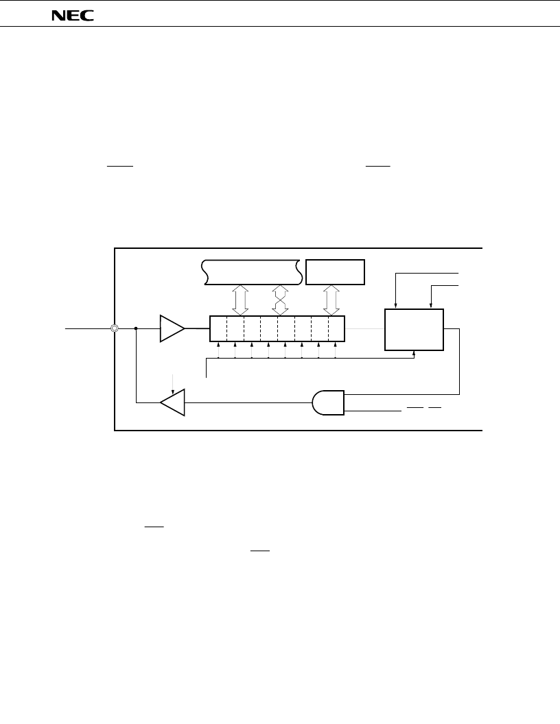
Shift register 0 (SIO0)
Fig. 4-42 shows a shift register 0 peripheral configuration. SIO0 is an 8-bit register which executes
parallel-to-serial conversion and carries out serial transmission/reception (shift operation) in synchro-
nization with a serial clock.
Serial transfer is started by writing data to SIO0.
In transmission, the data written to SIO0 is output to the serial output (SO0) or serial data bus
(SB0/SB1).
In reception, data is read from the serial input (SI0) or SB0/SB1 to SIO0.
This register can be read/written by an 8-bit manipulation instruction.
RESET input during operation makes the SIO0 value undefined. RESET input in the standby mode
holds the SIO0 value.
Shift operation stops after 8-bit transmission /reception.
Fig. 4-42 Shift Register 0 peripheral Configuration
SIO0 read and serial transfer start (write) are enabled at the following timings.
Serial interface operation enable/disable bit (CSIE0) = 1 except when CSIE0 is set to “1”
after data write to the shift register.
When the serial clock is masked after 8-bit serial transfer.
When SCK0 is at a high level
Be sure to write/read data to SIO0 when SCK0 is at a high level.
In the 2-wire serial I/O or SBI mode, the data bus has a configuration that the input pins
serve as output pins and vice versa. Each output pin has an N-ch open drain configuration.
Thus, set FFH to SIO0 for the device for data reception.
Internal Bus
Address
Comparator
Shift
Register 0
Shift Clock
N-ch Open Drain Output
SO0 Latch
CLR
RELT
CMDT
SET
Q
D
CLK
BUSY/ACK
CSIM0
相關PDF資料 |
PDF描述 |
|---|---|
| UPD75516 | 4-BIT, SINGLE-CHIP CMOS MICROCOMPUTER WITH EXTENSIVE I/O AND A/D CONVERTER |
| UPD75516GF-637-3B9 | 4-BIT SINGLE-CHIP MICROCOMPUTER |
| UPD75516GF-076 | 4-BIT SINGLE-CHIP MICROCOMPUTER |
| UPD75516GF-079 | 4-BIT SINGLE-CHIP MICROCOMPUTER |
| UPD75516GF-102 | 4-BIT SINGLE-CHIP MICROCOMPUTER |
相關代理商/技術參數 |
參數描述 |
|---|---|
| UPD753012AGC-P33-8BT-A | 制造商:Renesas Electronics Corporation 功能描述: |
| UPD753016AGC-P29-8BT | 制造商:Renesas Electronics Corporation 功能描述: |
| UPD75304GF-407-3B9 | 制造商:Renesas Electronics Corporation 功能描述: |
| UPD75306G182 | 制造商:Panasonic Industrial Company 功能描述:IC |
| UPD75308F478 | 制造商:Panasonic Industrial Company 功能描述:IC |
發(fā)布緊急采購,3分鐘左右您將得到回復。