- 您現(xiàn)在的位置:買(mǎi)賣(mài)IC網(wǎng) > PDF目錄383983 > UPD75236 (NEC Corp.) 4-BIT SINGLE-CHIP MICROCOMPUTER PDF資料下載
參數(shù)資料
| 型號(hào): | UPD75236 |
| 廠商: | NEC Corp. |
| 英文描述: | 4-BIT SINGLE-CHIP MICROCOMPUTER |
| 中文描述: | 4位單片機(jī) |
| 文件頁(yè)數(shù): | 171/190頁(yè) |
| 文件大小: | 1220K |
| 代理商: | UPD75236 |
第1頁(yè)第2頁(yè)第3頁(yè)第4頁(yè)第5頁(yè)第6頁(yè)第7頁(yè)第8頁(yè)第9頁(yè)第10頁(yè)第11頁(yè)第12頁(yè)第13頁(yè)第14頁(yè)第15頁(yè)第16頁(yè)第17頁(yè)第18頁(yè)第19頁(yè)第20頁(yè)第21頁(yè)第22頁(yè)第23頁(yè)第24頁(yè)第25頁(yè)第26頁(yè)第27頁(yè)第28頁(yè)第29頁(yè)第30頁(yè)第31頁(yè)第32頁(yè)第33頁(yè)第34頁(yè)第35頁(yè)第36頁(yè)第37頁(yè)第38頁(yè)第39頁(yè)第40頁(yè)第41頁(yè)第42頁(yè)第43頁(yè)第44頁(yè)第45頁(yè)第46頁(yè)第47頁(yè)第48頁(yè)第49頁(yè)第50頁(yè)第51頁(yè)第52頁(yè)第53頁(yè)第54頁(yè)第55頁(yè)第56頁(yè)第57頁(yè)第58頁(yè)第59頁(yè)第60頁(yè)第61頁(yè)第62頁(yè)第63頁(yè)第64頁(yè)第65頁(yè)第66頁(yè)第67頁(yè)第68頁(yè)第69頁(yè)第70頁(yè)第71頁(yè)第72頁(yè)第73頁(yè)第74頁(yè)第75頁(yè)第76頁(yè)第77頁(yè)第78頁(yè)第79頁(yè)第80頁(yè)第81頁(yè)第82頁(yè)第83頁(yè)第84頁(yè)第85頁(yè)第86頁(yè)第87頁(yè)第88頁(yè)第89頁(yè)第90頁(yè)第91頁(yè)第92頁(yè)第93頁(yè)第94頁(yè)第95頁(yè)第96頁(yè)第97頁(yè)第98頁(yè)第99頁(yè)第100頁(yè)第101頁(yè)第102頁(yè)第103頁(yè)第104頁(yè)第105頁(yè)第106頁(yè)第107頁(yè)第108頁(yè)第109頁(yè)第110頁(yè)第111頁(yè)第112頁(yè)第113頁(yè)第114頁(yè)第115頁(yè)第116頁(yè)第117頁(yè)第118頁(yè)第119頁(yè)第120頁(yè)第121頁(yè)第122頁(yè)第123頁(yè)第124頁(yè)第125頁(yè)第126頁(yè)第127頁(yè)第128頁(yè)第129頁(yè)第130頁(yè)第131頁(yè)第132頁(yè)第133頁(yè)第134頁(yè)第135頁(yè)第136頁(yè)第137頁(yè)第138頁(yè)第139頁(yè)第140頁(yè)第141頁(yè)第142頁(yè)第143頁(yè)第144頁(yè)第145頁(yè)第146頁(yè)第147頁(yè)第148頁(yè)第149頁(yè)第150頁(yè)第151頁(yè)第152頁(yè)第153頁(yè)第154頁(yè)第155頁(yè)第156頁(yè)第157頁(yè)第158頁(yè)第159頁(yè)第160頁(yè)第161頁(yè)第162頁(yè)第163頁(yè)第164頁(yè)第165頁(yè)第166頁(yè)第167頁(yè)第168頁(yè)第169頁(yè)第170頁(yè)當(dāng)前第171頁(yè)第172頁(yè)第173頁(yè)第174頁(yè)第175頁(yè)第176頁(yè)第177頁(yè)第178頁(yè)第179頁(yè)第180頁(yè)第181頁(yè)第182頁(yè)第183頁(yè)第184頁(yè)第185頁(yè)第186頁(yè)第187頁(yè)第188頁(yè)第189頁(yè)第190頁(yè)
171
μ
PD75236
MAIN SYSTEM CLOCK OSCILLATOR CHARACTERISTICS (Ta = –40 to +85
°
C, V
DD
= 2.7 to 6.0 V )
UNIT
MAX.
TYP.
UNIT
MAX.
TYP.
MIN.
PARAMETER
TEST CONDITIONS
MIN.
V
DD
= Oscillation
voltage range
After V
DD
reaches the
minimum value in
the oscillation
voltage range
V
DD
= 4.5 to 6.0 V
Oscillator frequency
(f
X
)
*1
Oscillation
stabilization time
*2
Oscillator frequency
(f
X
)
*1
Oscillation stabilization
time
*2
X1 input frequency
(f
X
)
*1
X1 high and low level
widths (t
XH
, t
XL
)
X1
X2
C1
C2
X1
X2
C1
C2
* 1.
Oscillator characteristics only. Refer to the description of AC characteristics for details of instruction
execution time.
Time required for oscillation to become stabilized after V
DD
application or STOP mode release.
When oscillation frequency is " 4.19 < f
X
≤
5.0 MHz ", do not select " PCC = 0011 " as instruction execution
time. If " PCC = 0011 " is selected, 1 machine cycle becomes less than 0.95
μ
s, with the result that the
specified MIN. value of 0.95
μ
s cannot be observed.
2.
3.
SUBSYSTEM CLOCK OSCILLATOR CHARACTERISTICS (Ta = –40 to +85
°
C, V
DD
= 2.7 to 6.0 V)
* 1.
Oscillator characteristics only. Refer to the description of AC characteristics for instruction execution
time.
Time required for oscillation to become stabilized after V
DD
application or STOP mode release.
2.
XT1
XT2
C3
C4
R
PARAMETER
TEST CONDITIONS
Oscillator frequency
(f
XT
)
*1
Oscillation stabilization
time
*2
XT1 input frequency
(f
XT
)
*1
XT1 high and low level
widths (t
XTH
, t
XTL
)
X1
X2
μ
PD74HCU04
XT1
XT2
#
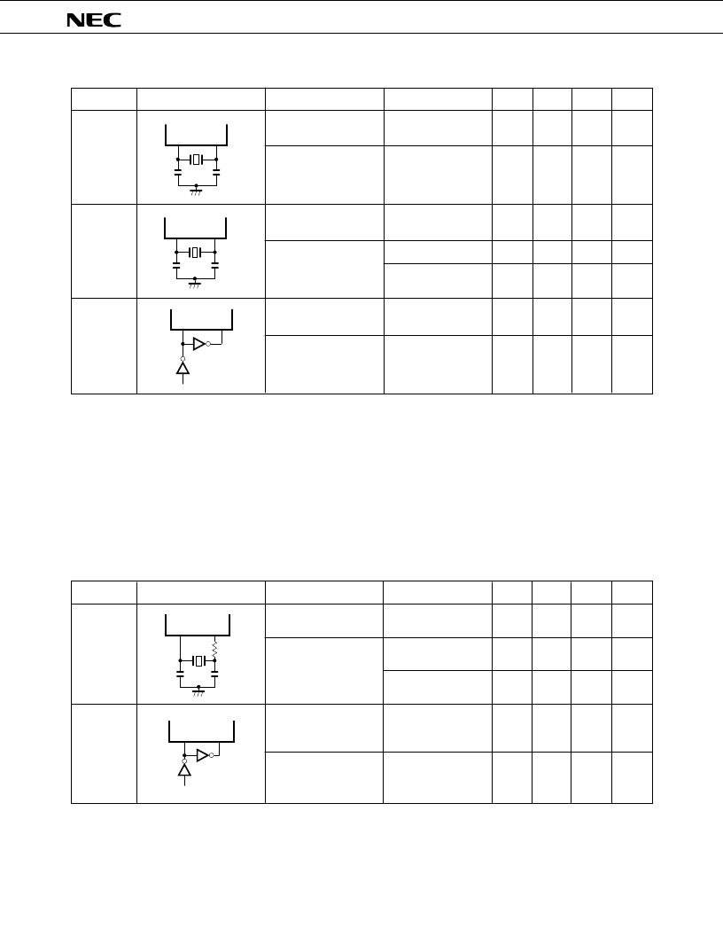
RESONATOR RECOMMENDED CIRCUIT
RESONATOR RECOMMENDED CIRCUIT
2.0
2.0
2.0
100
Ceramic
resonator
Crystal
resonator
External
clock
4.19
5.0
4
5.0
*3
10
30
5.0
250
MHz
ms
MHz
ms
ms
MHz
ns
Crystal
resonator
External
clock
V
DD
= 4.5 to 6.0 V
32
32
5
32.768
1.0
35
2
10
100
15
kHz
s
s
kHz
μ
s
相關(guān)PDF資料 |
PDF描述 |
|---|---|
| UPD75516 | 4-BIT, SINGLE-CHIP CMOS MICROCOMPUTER WITH EXTENSIVE I/O AND A/D CONVERTER |
| UPD75516GF-637-3B9 | 4-BIT SINGLE-CHIP MICROCOMPUTER |
| UPD75516GF-076 | 4-BIT SINGLE-CHIP MICROCOMPUTER |
| UPD75516GF-079 | 4-BIT SINGLE-CHIP MICROCOMPUTER |
| UPD75516GF-102 | 4-BIT SINGLE-CHIP MICROCOMPUTER |
相關(guān)代理商/技術(shù)參數(shù) |
參數(shù)描述 |
|---|---|
| UPD753012AGC-P33-8BT-A | 制造商:Renesas Electronics Corporation 功能描述: |
| UPD753016AGC-P29-8BT | 制造商:Renesas Electronics Corporation 功能描述: |
| UPD75304GF-407-3B9 | 制造商:Renesas Electronics Corporation 功能描述: |
| UPD75306G182 | 制造商:Panasonic Industrial Company 功能描述:IC |
| UPD75308F478 | 制造商:Panasonic Industrial Company 功能描述:IC |
發(fā)布緊急采購(gòu),3分鐘左右您將得到回復(fù)。