- 您現(xiàn)在的位置:買賣IC網(wǎng) > PDF目錄383961 > TMX320DM6437BZWTA (Texas Instruments, Inc.) Digital Media Processor PDF資料下載
參數(shù)資料
| 型號(hào): | TMX320DM6437BZWTA |
| 廠商: | Texas Instruments, Inc. |
| 英文描述: | Digital Media Processor |
| 中文描述: | 數(shù)字媒體處理器 |
| 文件頁(yè)數(shù): | 202/309頁(yè) |
| 文件大小: | 2216K |
| 代理商: | TMX320DM6437BZWTA |
第1頁(yè)第2頁(yè)第3頁(yè)第4頁(yè)第5頁(yè)第6頁(yè)第7頁(yè)第8頁(yè)第9頁(yè)第10頁(yè)第11頁(yè)第12頁(yè)第13頁(yè)第14頁(yè)第15頁(yè)第16頁(yè)第17頁(yè)第18頁(yè)第19頁(yè)第20頁(yè)第21頁(yè)第22頁(yè)第23頁(yè)第24頁(yè)第25頁(yè)第26頁(yè)第27頁(yè)第28頁(yè)第29頁(yè)第30頁(yè)第31頁(yè)第32頁(yè)第33頁(yè)第34頁(yè)第35頁(yè)第36頁(yè)第37頁(yè)第38頁(yè)第39頁(yè)第40頁(yè)第41頁(yè)第42頁(yè)第43頁(yè)第44頁(yè)第45頁(yè)第46頁(yè)第47頁(yè)第48頁(yè)第49頁(yè)第50頁(yè)第51頁(yè)第52頁(yè)第53頁(yè)第54頁(yè)第55頁(yè)第56頁(yè)第57頁(yè)第58頁(yè)第59頁(yè)第60頁(yè)第61頁(yè)第62頁(yè)第63頁(yè)第64頁(yè)第65頁(yè)第66頁(yè)第67頁(yè)第68頁(yè)第69頁(yè)第70頁(yè)第71頁(yè)第72頁(yè)第73頁(yè)第74頁(yè)第75頁(yè)第76頁(yè)第77頁(yè)第78頁(yè)第79頁(yè)第80頁(yè)第81頁(yè)第82頁(yè)第83頁(yè)第84頁(yè)第85頁(yè)第86頁(yè)第87頁(yè)第88頁(yè)第89頁(yè)第90頁(yè)第91頁(yè)第92頁(yè)第93頁(yè)第94頁(yè)第95頁(yè)第96頁(yè)第97頁(yè)第98頁(yè)第99頁(yè)第100頁(yè)第101頁(yè)第102頁(yè)第103頁(yè)第104頁(yè)第105頁(yè)第106頁(yè)第107頁(yè)第108頁(yè)第109頁(yè)第110頁(yè)第111頁(yè)第112頁(yè)第113頁(yè)第114頁(yè)第115頁(yè)第116頁(yè)第117頁(yè)第118頁(yè)第119頁(yè)第120頁(yè)第121頁(yè)第122頁(yè)第123頁(yè)第124頁(yè)第125頁(yè)第126頁(yè)第127頁(yè)第128頁(yè)第129頁(yè)第130頁(yè)第131頁(yè)第132頁(yè)第133頁(yè)第134頁(yè)第135頁(yè)第136頁(yè)第137頁(yè)第138頁(yè)第139頁(yè)第140頁(yè)第141頁(yè)第142頁(yè)第143頁(yè)第144頁(yè)第145頁(yè)第146頁(yè)第147頁(yè)第148頁(yè)第149頁(yè)第150頁(yè)第151頁(yè)第152頁(yè)第153頁(yè)第154頁(yè)第155頁(yè)第156頁(yè)第157頁(yè)第158頁(yè)第159頁(yè)第160頁(yè)第161頁(yè)第162頁(yè)第163頁(yè)第164頁(yè)第165頁(yè)第166頁(yè)第167頁(yè)第168頁(yè)第169頁(yè)第170頁(yè)第171頁(yè)第172頁(yè)第173頁(yè)第174頁(yè)第175頁(yè)第176頁(yè)第177頁(yè)第178頁(yè)第179頁(yè)第180頁(yè)第181頁(yè)第182頁(yè)第183頁(yè)第184頁(yè)第185頁(yè)第186頁(yè)第187頁(yè)第188頁(yè)第189頁(yè)第190頁(yè)第191頁(yè)第192頁(yè)第193頁(yè)第194頁(yè)第195頁(yè)第196頁(yè)第197頁(yè)第198頁(yè)第199頁(yè)第200頁(yè)第201頁(yè)當(dāng)前第202頁(yè)第203頁(yè)第204頁(yè)第205頁(yè)第206頁(yè)第207頁(yè)第208頁(yè)第209頁(yè)第210頁(yè)第211頁(yè)第212頁(yè)第213頁(yè)第214頁(yè)第215頁(yè)第216頁(yè)第217頁(yè)第218頁(yè)第219頁(yè)第220頁(yè)第221頁(yè)第222頁(yè)第223頁(yè)第224頁(yè)第225頁(yè)第226頁(yè)第227頁(yè)第228頁(yè)第229頁(yè)第230頁(yè)第231頁(yè)第232頁(yè)第233頁(yè)第234頁(yè)第235頁(yè)第236頁(yè)第237頁(yè)第238頁(yè)第239頁(yè)第240頁(yè)第241頁(yè)第242頁(yè)第243頁(yè)第244頁(yè)第245頁(yè)第246頁(yè)第247頁(yè)第248頁(yè)第249頁(yè)第250頁(yè)第251頁(yè)第252頁(yè)第253頁(yè)第254頁(yè)第255頁(yè)第256頁(yè)第257頁(yè)第258頁(yè)第259頁(yè)第260頁(yè)第261頁(yè)第262頁(yè)第263頁(yè)第264頁(yè)第265頁(yè)第266頁(yè)第267頁(yè)第268頁(yè)第269頁(yè)第270頁(yè)第271頁(yè)第272頁(yè)第273頁(yè)第274頁(yè)第275頁(yè)第276頁(yè)第277頁(yè)第278頁(yè)第279頁(yè)第280頁(yè)第281頁(yè)第282頁(yè)第283頁(yè)第284頁(yè)第285頁(yè)第286頁(yè)第287頁(yè)第288頁(yè)第289頁(yè)第290頁(yè)第291頁(yè)第292頁(yè)第293頁(yè)第294頁(yè)第295頁(yè)第296頁(yè)第297頁(yè)第298頁(yè)第299頁(yè)第300頁(yè)第301頁(yè)第302頁(yè)第303頁(yè)第304頁(yè)第305頁(yè)第306頁(yè)第307頁(yè)第308頁(yè)第309頁(yè)
www.ti.com
P
6.7.4
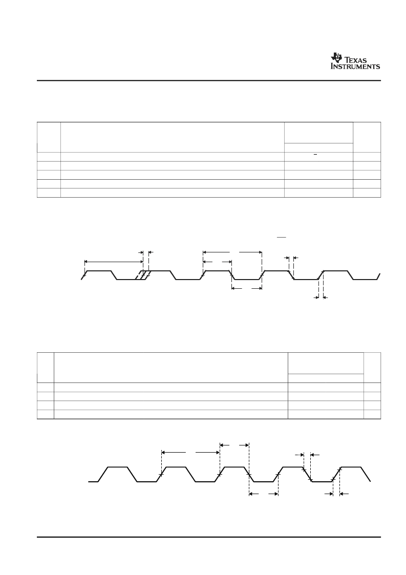
Clock PLL Electrical Data/Timing (Input and Output Clocks)
MXI/CLKIN
2
3
4
4
5
1
CLK_OUT0
(Divide-by-1)
4
4
2
1
3
TMS320DM6437
Digital Media Processor
SPRS345B–NOVEMBER 2006–REVISED MARCH 2007
Table 6-19. Timing Requirements for MXI/CLKIN (-400, -500, -600) Devices
(1)(2)(3)(4)
(see
Figure 6-12
)
-400
-500
-600
NO.
UNIT
MIN
33.3
0.45C
0.45C
MAX
1
2
3
4
5
t
c(MXI)
t
w(MXIH)
t
w(MXIL)
t
t(MXI)
t
J(MXI)
Cycle time, MXI/CLKIN
Pulse duration, MXI/CLKIN high
Pulse duration, MXI/CLKIN low
Transition time, MXI/CLKIN
Period jitter, MXI/CLKIN
50
ns
ns
ns
ns
ns
0.55C
0.55C
0.05C
0.02C
(1)
The MXI/CLKIN frequency and PLL multiply factor should be chosen such that the resulting clock frequency is within the specific range
for CPU operating frequency. For example, for a -600 speed device with a 27 MHz CLKIN frequency, the PLL multiply factor should be
≤
22.
The reference points for the rise and fall transitions are measured at V
MAX and V
MIN.
For more details on the PLL multiplier factors, see the
Documentation Support
section for the TMS320DM63x DMP DSP Subsystem
Reference Guide (Literature Number SPRU978).
C = CLKIN cycle time in ns. For example, when MXI/CLKIN frequency is 27 MHz, use C = 37.037 ns.
(2)
(3)
(4)
Figure 6-12. MXI/CLKIN Timing
Table 6-20. Switching Characteristics Over Recommended Operating Conditions for CLKOUT0
(1)(2)
(see
Figure 6-13
)
-400
-500
-600
NO.
PARAMETER
UNIT
MIN
33.3
0.45P
0.45P
MAX
1
2
3
4
t
C
t
w(CLKOUT0H)
t
w(CLKOUT0L)
t
t(CLKOUT0)
The reference points for the rise and fall transitions are measured at V
MAX and V
MIN.
P = 1/CLKOUT0 clock frequency in nanoseconds (ns). For example, when CLKOUT0 frequency is 27 MHz, use P = 37.04 ns.
Cycle time, CLKOUT0
Pulse duration, CLKOUT0 high
Pulse duration, CLKOUT0 low
Transition time, CLKOUT0
50
ns
ns
ns
ns
0.55P
0.55P
0.05P
(1)
(2)
Figure 6-13. CLKOUT0 Timing
202
Peripheral Information and Electrical Specifications
Submit Documentation Feedback
相關(guān)PDF資料 |
PDF描述 |
|---|---|
| TMS320DM6443_07 | Digital Media System-on-Chip |
| TMX320DM6443AZWT | Digital Media System-on-Chip |
| TMX320DM6443ZWT | Digital Media System-on-Chip |
| TMS320DM647_08 | Digital Media Processor |
| TMS320DM647ZUT720 | Digital Media Processor |
相關(guān)代理商/技術(shù)參數(shù) |
參數(shù)描述 |
|---|---|
| TMX320DM6441CZWT | 制造商:Texas Instruments 功能描述: |
| TMX320DM6441DZWT | 制造商:Texas Instruments 功能描述:DAVINCI DIGITAL MEDIA SYSTEM-ON-CHIP - Tape and Reel |
| TMX320DM6443AZWT | 制造商:Rochester Electronics LLC 功能描述:DAVINCI DIGITAL MEDIA SYSTEM-ON-CHIP - Tape and Reel |
| TMX320DM6443BZWT | 制造商:Texas Instruments 功能描述: |
| TMX320DM6443CZWT | 制造商:Texas Instruments 功能描述: |
發(fā)布緊急采購(gòu),3分鐘左右您將得到回復(fù)。