- 您現(xiàn)在的位置:買賣IC網(wǎng) > PDF目錄382635 > TMS320C241PGS 16-Bit Digital Signal Processor PDF資料下載
參數(shù)資料
| 型號: | TMS320C241PGS |
| 元件分類: | 數(shù)字信號處理 |
| 英文描述: | 16-Bit Digital Signal Processor |
| 中文描述: | 16位數(shù)字信號處理器 |
| 文件頁數(shù): | 101/116頁 |
| 文件大小: | 1485K |
| 代理商: | TMS320C241PGS |
第1頁第2頁第3頁第4頁第5頁第6頁第7頁第8頁第9頁第10頁第11頁第12頁第13頁第14頁第15頁第16頁第17頁第18頁第19頁第20頁第21頁第22頁第23頁第24頁第25頁第26頁第27頁第28頁第29頁第30頁第31頁第32頁第33頁第34頁第35頁第36頁第37頁第38頁第39頁第40頁第41頁第42頁第43頁第44頁第45頁第46頁第47頁第48頁第49頁第50頁第51頁第52頁第53頁第54頁第55頁第56頁第57頁第58頁第59頁第60頁第61頁第62頁第63頁第64頁第65頁第66頁第67頁第68頁第69頁第70頁第71頁第72頁第73頁第74頁第75頁第76頁第77頁第78頁第79頁第80頁第81頁第82頁第83頁第84頁第85頁第86頁第87頁第88頁第89頁第90頁第91頁第92頁第93頁第94頁第95頁第96頁第97頁第98頁第99頁第100頁當(dāng)前第101頁第102頁第103頁第104頁第105頁第106頁第107頁第108頁第109頁第110頁第111頁第112頁第113頁第114頁第115頁第116頁
TMS320F243, TMS320F241
DSP CONTROLLERS
SPRS064B – DECEMBER 1997 – REVISED FEBRUARY 1999
101
POST OFFICE BOX 1443
HOUSTON, TEXAS 77251–1443
operating characteristics over recommended operating condition ranges
PARAMETER
DESCRIPTION
MIN
MAX
UNIT
VCCA= 5 5 V
VCCA = 5.5 V
Converting
10
mA
ICCA
Analog supply current
Non-converting
2
VCCA = VREFHI = 5.5 V
PLL or OSC power
down
1
A
Ci
Cai
Analog input capacitance
Typical capacitive load on
analog input pin
Non-sampling
10
pF
Sampling
30
EDNL
Differential nonlinearity error
Difference between the actual step width and the ideal
value
2
LSB
EINL
Integral nonlinearity error
Maximum deviation from the best straight line through
the ADC transfer characteristics, excluding the
quantization error
2
LSB
td(PU)
Delay time, power-up to ADC valid
Time to stabilize analog stage after power-up
10
s
ZAI
Analog input source impedance
Analog input source impedance for conversions to
remain within specifications
10
Absolute resolution = 4.89 mV. At VREFHI = 5 V and VREFLO = 0 V, this s one LSB. As VREFHI decreases, VREFLO ncreases, or both, the LSB size
decreases. Therefore, the absolute accuracy and differential/integral linearity errors in terms of LSBs increase.
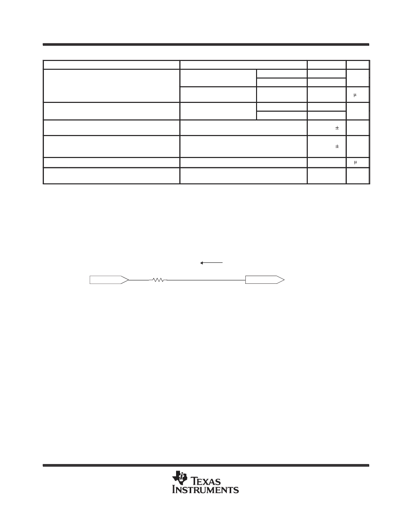
ADC input pin circuit
One of the most common A/D application errors is inappropriate source impedance. In practice, minimum
source impedance should be used to limit the error as well as to minimize the required sampling time; however,
the source impedance must be smaller than Z
AI
. A typical ADC input pin circuit is shown in Figure 42.
VIN
R1
Requiv
VAI
(to ADCINx input)
R1 = 10
typical
Figure 42. Typical ADC Input Pin Circuit
相關(guān)PDF資料 |
PDF描述 |
|---|---|
| TMS320F241FNQ | 16-Bit Digital Signal Processor |
| TMS320F241PGQ | 16-Bit Digital Signal Processor |
| TMS320F243PGEQ | 16-Bit Digital Signal Processor |
| TMS320F243PGES | 16-Bit Digital Signal Processor |
| TMS320C3X | 32-Bit Digital Signal Processor |
相關(guān)代理商/技術(shù)參數(shù) |
參數(shù)描述 |
|---|---|
| TMS320C242 | 制造商:TI 制造商全稱:Texas Instruments 功能描述:DSP CONTROLLER |
| TMS320C242FN | 制造商:TI 制造商全稱:Texas Instruments 功能描述:DSP CONTROLLER |
| TMS320C242FNA | 制造商:未知廠家 制造商全稱:未知廠家 功能描述:16-Bit Digital Signal Processor |
| TMS320C242FNS | 制造商:未知廠家 制造商全稱:未知廠家 功能描述:16-Bit Digital Signal Processor |
| TMS320C242PG | 制造商:TI 制造商全稱:Texas Instruments 功能描述:DSP CONTROLLER |
發(fā)布緊急采購,3分鐘左右您將得到回復(fù)。