- 您現(xiàn)在的位置:買賣IC網(wǎng) > PDF目錄384004 > TLC320AD55C (Texas Instruments, Inc.) Sigma-Delta Analog Interface Circuit(Sigma-Delta 模擬接口) PDF資料下載
參數(shù)資料
| 型號(hào): | TLC320AD55C |
| 廠商: | Texas Instruments, Inc. |
| 英文描述: | Sigma-Delta Analog Interface Circuit(Sigma-Delta 模擬接口) |
| 中文描述: | sigma - delta模擬接口電路(Σ-Δ模擬接口) |
| 文件頁數(shù): | 27/41頁 |
| 文件大小: | 256K |
| 代理商: | TLC320AD55C |
第1頁第2頁第3頁第4頁第5頁第6頁第7頁第8頁第9頁第10頁第11頁第12頁第13頁第14頁第15頁第16頁第17頁第18頁第19頁第20頁第21頁第22頁第23頁第24頁第25頁第26頁當(dāng)前第27頁第28頁第29頁第30頁第31頁第32頁第33頁第34頁第35頁第36頁第37頁第38頁第39頁第40頁第41頁
4–1
4 Specifications
4.1
Absolute Maximum Ratings Over Operating Free-Air Temperature Range
(unless otherwise noted)
Supply voltage range, DV
DD,
V
DD
(ADC, DAC)(see Note 1)
Output voltage range, DOUT, FS, SCLK, FLAG 0, FLAG 1
Output voltage range, OUTP, OUTM
Input voltage range, DIN, PWRDWN, RESET, ALT DATA,
MCLK, FC
. . . . . . . . . . . . . . . . . . . . . . . . . . . . . . . . . . . . . . . . . . .
Input voltage range, INP, INM, AUXP, AUXM
Case temperature for 10 seconds, T
C
: DW package
Operating free-air temperature range, T
A
Storage temperature range, T
stg
Stresses beyond those listed under “absolute maximum ratings” may cause permanent damage to the device. These
are stress ratings only, and functional operation of the device at these or any other conditions beyond those indicated
under “recommended operating conditions” is not implied. Exposure to absolute-maximum-rated conditions for
extended periods may affect device reliability.
NOTE 1: All voltage values are with respect to VSS(DAC) for DAC channel measurements and VSS(ADC) for ADC
channel measurements.
–0.3 V to 6.5 V
. . . . . . . . . .
–0.3 V to DV
DD
+ 0.3 V
. . .
–0.3 V to V
DD
+ 0.3 V
. . . . . . . . . . . . . . . . . . . . . . . .
–0.3 V to DV
DD
+ 0.3 V
–0.3 V to V
DD
+ 0.3 V
. . . . . . . . . . . . . . . . . . . . . . . . .
. . . . . . . . . . . . . . . . . . . . . . . . . . . .
. . . . . . . . . . . . . . . . . . . . . . . . . . . . . . . . .
. . . . . . . . . . . . . . . .
260
°
C
0
°
C to 70
°
C
–65
°
C to 150
°
C
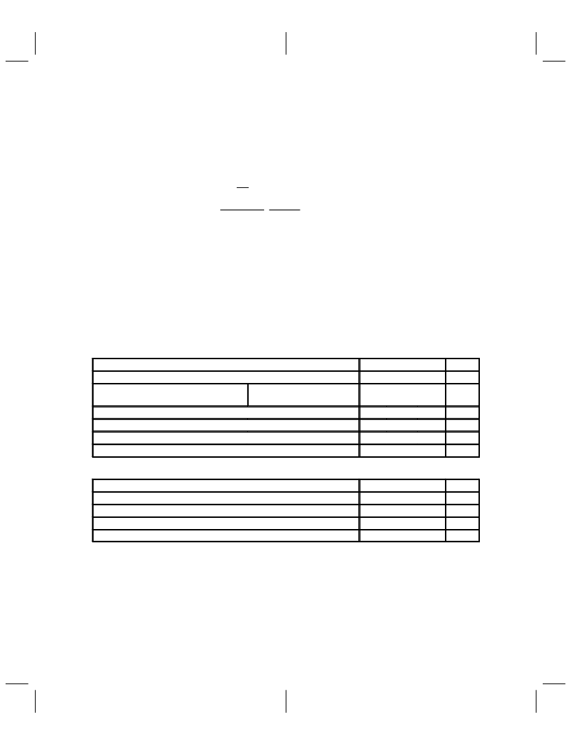
4.2
Recommended Operating Conditions
MIN
NOM
MAX
UNIT
Supply voltage, VDD(ADC, DAC)
4.5
5.5
V
Analog signal input voltage, VI
Differential, (INP–INM) peak,
for full scale operation
6
V
Load resistance for OUTP and OUTM, RL
Load capacitance for OUTP and OUTM, CL
ADC or DAC conversion rate (Nyquist)
0.3
10
k
pF
100
8
kHz
°
C
Operating free-air temperature, TA
0
70
4.3
Recommended Operating Conditions
,
DV
DD
= 5 V
MIN
NOM
MAX
UNIT
Supply voltage, DVDD
High-level input voltage, VIH
Low-level input voltage, VIL
MCLK frequency (see Note 2), duty cycle = 50
±
10%
NOTE 2: The default state for an 8 kHz conversion rate requires a 16.384 MHz MCLK frequency.
4.5
5.5
V
2
V
0.8
V
16.384
MHz
相關(guān)PDF資料 |
PDF描述 |
|---|---|
| TLC320AD56(中文) | Sigma-Delta Analog Interface Circuit(Sigma-Delta 模擬接口) |
| TLC320AD56C | Sigma-Delta Analog Interface Circuit |
| tlc320ad56c | Sigma-Delta Analog Interface Circuit(Sigma-Delta 模擬接口電路) |
| TLC320AD57(中文) | Sigma-Delta Analog Interface Circuit(Sigma-Delta立體聲音頻ADC) |
| TLC320AD57C | Sigma-Delta Stereo Analog-to-Digital Converter |
相關(guān)代理商/技術(shù)參數(shù) |
參數(shù)描述 |
|---|---|
| TLC320AD56 | 制造商:TI 制造商全稱:Texas Instruments 功能描述:Sigma-Delta Analog Interface Circuit |
| TLC320AD56C | 制造商:TI 制造商全稱:Texas Instruments 功能描述:Sigma-Delta Analog Interface Circuit |
| TLC320AD56CFN | 制造商:Rochester Electronics LLC 功能描述:- Bulk 制造商:Texas Instruments 功能描述: |
| TLC320AD56CPT | 制造商:Rochester Electronics LLC 功能描述:- Bulk 制造商:Texas Instruments 功能描述: |
| TLC320AD57 | 制造商:TI 制造商全稱:Texas Instruments 功能描述:Sigma-Delta Stereo Analog-to-Digital Converter |
發(fā)布緊急采購,3分鐘左右您將得到回復(fù)。