- 您現(xiàn)在的位置:買賣IC網(wǎng) > PDF目錄98143 > ST52510F3M6 (STMICROELECTRONICS) MICROCONTROLLER, PDSO20 PDF資料下載
參數(shù)資料
| 型號(hào): | ST52510F3M6 |
| 廠商: | STMICROELECTRONICS |
| 元件分類: | 微控制器/微處理器 |
| 英文描述: | MICROCONTROLLER, PDSO20 |
| 封裝: | SOP-20 |
| 文件頁(yè)數(shù): | 66/136頁(yè) |
| 文件大小: | 3335K |
| 代理商: | ST52510F3M6 |
第1頁(yè)第2頁(yè)第3頁(yè)第4頁(yè)第5頁(yè)第6頁(yè)第7頁(yè)第8頁(yè)第9頁(yè)第10頁(yè)第11頁(yè)第12頁(yè)第13頁(yè)第14頁(yè)第15頁(yè)第16頁(yè)第17頁(yè)第18頁(yè)第19頁(yè)第20頁(yè)第21頁(yè)第22頁(yè)第23頁(yè)第24頁(yè)第25頁(yè)第26頁(yè)第27頁(yè)第28頁(yè)第29頁(yè)第30頁(yè)第31頁(yè)第32頁(yè)第33頁(yè)第34頁(yè)第35頁(yè)第36頁(yè)第37頁(yè)第38頁(yè)第39頁(yè)第40頁(yè)第41頁(yè)第42頁(yè)第43頁(yè)第44頁(yè)第45頁(yè)第46頁(yè)第47頁(yè)第48頁(yè)第49頁(yè)第50頁(yè)第51頁(yè)第52頁(yè)第53頁(yè)第54頁(yè)第55頁(yè)第56頁(yè)第57頁(yè)第58頁(yè)第59頁(yè)第60頁(yè)第61頁(yè)第62頁(yè)第63頁(yè)第64頁(yè)第65頁(yè)當(dāng)前第66頁(yè)第67頁(yè)第68頁(yè)第69頁(yè)第70頁(yè)第71頁(yè)第72頁(yè)第73頁(yè)第74頁(yè)第75頁(yè)第76頁(yè)第77頁(yè)第78頁(yè)第79頁(yè)第80頁(yè)第81頁(yè)第82頁(yè)第83頁(yè)第84頁(yè)第85頁(yè)第86頁(yè)第87頁(yè)第88頁(yè)第89頁(yè)第90頁(yè)第91頁(yè)第92頁(yè)第93頁(yè)第94頁(yè)第95頁(yè)第96頁(yè)第97頁(yè)第98頁(yè)第99頁(yè)第100頁(yè)第101頁(yè)第102頁(yè)第103頁(yè)第104頁(yè)第105頁(yè)第106頁(yè)第107頁(yè)第108頁(yè)第109頁(yè)第110頁(yè)第111頁(yè)第112頁(yè)第113頁(yè)第114頁(yè)第115頁(yè)第116頁(yè)第117頁(yè)第118頁(yè)第119頁(yè)第120頁(yè)第121頁(yè)第122頁(yè)第123頁(yè)第124頁(yè)第125頁(yè)第126頁(yè)第127頁(yè)第128頁(yè)第129頁(yè)第130頁(yè)第131頁(yè)第132頁(yè)第133頁(yè)第134頁(yè)第135頁(yè)第136頁(yè)
Obsolete
Product(s)
- Obsolete
Product(s)
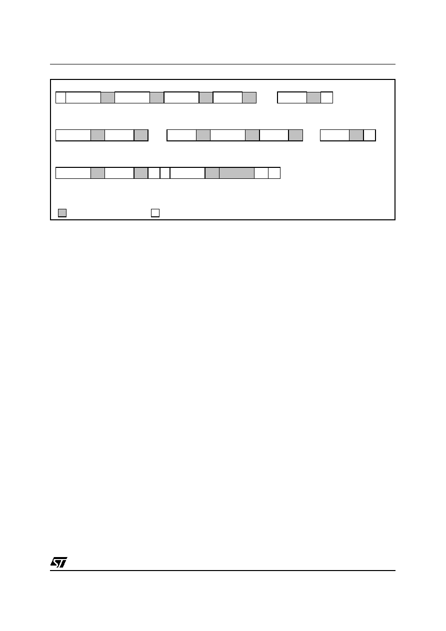
Figure 4.1 Commands and Data Communication Sequences
The generic procedure of commands execution,
with the data communication in both directions is
displayed in Figure 4.1.
Remark: the Slave Address 1010000 must be sent
after a Stop (i.e. each time the data direction
changes, to specify the R/W bit). For example: if a
command to send data to the device has been
executed, a command for receiving data must be
followed by the slave address and the R/W bit must
be set to 1. The Programming Mode code doesn’t
need to be specified again.
Warning: After entering the Programming Mode,
the currently pointed address is the Page 48, Block
3, byte 0 (Lock Byte).
The
list
of
the
available
commands
in
Programming Mode is showed in Table 4.2
4.2.2 Fast Programming procedure. The
fastest way to program the device memory is the
use of the FastBlockWrite command. The following
procedure can be used to write the memory with a
new program and new data, starting from the first
memory location:
1.
The Programming Mode is entered with the
sequence described above
2.
The memory is erased (all bits are put to 0)
with the GlobalErase command. The device
holds the SCL line low, releasing it after the
command is completed (about 2 ms). This
command also unlocks the device if locked.
3.
The FastBlockWrite command is sent and the
device acknowledges it
4.
The 32 bytes of data to be written in the first
memory Block are sent in a sequence. The
device acknowledges each of them
5.
After the device acknowledges the 32nd byte,
it holds the SCL line until the parallel writing of
the 32 byte is completed (about 2.5 ms)
6.
The Block Pointer is incremented by sending
the IncBlock command
7.
The procedure is repeated from point 3 until
there is data to be sent to the memory
Note: the Block Pointer assumes values between
0 to 7 (there are 8 blocks in a page). When the
Block Pointer is equal to 7, the IncBlock command
puts this pointer to 0 and increments the Page
Pointer. The Page Pointer, after page writing is
completed, doesn’t have to be incremented in the
procedure above described.
4.2.3 Random data writing. A single byte can be
written in a specified memory location by using the
following procedure:
1.
The Programming Mode is entered with the
sequence described in Section 4.2.1
2.
The SetPage command is sent, followed by
the page number where the data should be
written
3.
The ByteWrite command is sent followed by
two bytes
4.
The first bytes that follows the ByteWrite com-
mand is the address inside the pointed page
where the data must be written.
5.
The second byte is the data to be written
6.
The device held the SCL line low until the data
is not stored in the memory (about 4.5 ms: 2
ms for erasing and 2.5 for writing)
Programming mode start sequence
Execution of commands for writing data:
Execution of commands for reading data:
S=Start, P=Stop, A=Acknowledge, NA=Non-acknowledge
From Slave to Master
From Master to Slave
S 10100000
A
00000000
A
Command
A
Data1
A
.....
DataN
AP
Command
A
Data1
A
.....
DataN
A
Command
A
Data1
A
.....
DataN
AP
Command
A
Address
A
P
S 10100001
A
Data read NA
P
相關(guān)PDF資料 |
PDF描述 |
|---|---|
| ST52E430B/D | 8-BIT, UVPROM, 20 MHz, MICROCONTROLLER, CDIP32 |
| ST52F510F1M6 | 8-BIT, FLASH, 24 MHz, MICROCONTROLLER, PDSO20 |
| ST52F510G0B6 | 8-BIT, FLASH, 24 MHz, MICROCONTROLLER, PDIP28 |
| ST52F513F0M6 | 8-BIT, FLASH, 24 MHz, MICROCONTROLLER, PDSO20 |
| ST52F513F1B6 | 8-BIT, FLASH, 24 MHz, MICROCONTROLLER, PDIP20 |
相關(guān)代理商/技術(shù)參數(shù) |
參數(shù)描述 |
|---|---|
| ST52510G2 | 制造商:未知廠家 制造商全稱:未知廠家 功能描述:8-BIT ICU WITH 10-BIT ADC. TWO TIMERS/PWM. I2C. SPI. SCI. UP TO 8K FLASH |
| ST52510G3 | 制造商:未知廠家 制造商全稱:未知廠家 功能描述:8-BIT ICU WITH 10-BIT ADC. TWO TIMERS/PWM. I2C. SPI. SCI. UP TO 8K FLASH |
| ST52510K2 | 制造商:未知廠家 制造商全稱:未知廠家 功能描述:8-BIT ICU WITH 10-BIT ADC. TWO TIMERS/PWM. I2C. SPI. SCI. UP TO 8K FLASH |
| ST52510K3 | 制造商:未知廠家 制造商全稱:未知廠家 功能描述:8-BIT ICU WITH 10-BIT ADC. TWO TIMERS/PWM. I2C. SPI. SCI. UP TO 8K FLASH |
| ST52510Y2 | 制造商:未知廠家 制造商全稱:未知廠家 功能描述:8-BIT ICU WITH 10-BIT ADC. TWO TIMERS/PWM. I2C. SPI. SCI. UP TO 8K FLASH |
發(fā)布緊急采購(gòu),3分鐘左右您將得到回復(fù)。