- 您現(xiàn)在的位置:買賣IC網(wǎng) > PDF目錄98143 > ST52510F3M6 (STMICROELECTRONICS) MICROCONTROLLER, PDSO20 PDF資料下載
參數(shù)資料
| 型號: | ST52510F3M6 |
| 廠商: | STMICROELECTRONICS |
| 元件分類: | 微控制器/微處理器 |
| 英文描述: | MICROCONTROLLER, PDSO20 |
| 封裝: | SOP-20 |
| 文件頁數(shù): | 101/136頁 |
| 文件大小: | 3335K |
| 代理商: | ST52510F3M6 |
第1頁第2頁第3頁第4頁第5頁第6頁第7頁第8頁第9頁第10頁第11頁第12頁第13頁第14頁第15頁第16頁第17頁第18頁第19頁第20頁第21頁第22頁第23頁第24頁第25頁第26頁第27頁第28頁第29頁第30頁第31頁第32頁第33頁第34頁第35頁第36頁第37頁第38頁第39頁第40頁第41頁第42頁第43頁第44頁第45頁第46頁第47頁第48頁第49頁第50頁第51頁第52頁第53頁第54頁第55頁第56頁第57頁第58頁第59頁第60頁第61頁第62頁第63頁第64頁第65頁第66頁第67頁第68頁第69頁第70頁第71頁第72頁第73頁第74頁第75頁第76頁第77頁第78頁第79頁第80頁第81頁第82頁第83頁第84頁第85頁第86頁第87頁第88頁第89頁第90頁第91頁第92頁第93頁第94頁第95頁第96頁第97頁第98頁第99頁第100頁當(dāng)前第101頁第102頁第103頁第104頁第105頁第106頁第107頁第108頁第109頁第110頁第111頁第112頁第113頁第114頁第115頁第116頁第117頁第118頁第119頁第120頁第121頁第122頁第123頁第124頁第125頁第126頁第127頁第128頁第129頁第130頁第131頁第132頁第133頁第134頁第135頁第136頁
Obsolete
Product(s)
- Obsolete
Product(s)
10 10-BIT A/D CONVERTER
10.1 Introduction
ST52F510/F513 A/D Converter is a 10-bit analog
to digital converter with up to 8 analog inputs. The
A/D converter offers a typical conversion time of 10
μs in fast mode and of 20 μs in slow mode. This
period also includes the time of the integral Sample
and Hold circuitry, which minimizes the need for
external components and allows quick sampling of
the signal for the minimum warping effect and
integral conversion error.
In addition the peripheral performs a calibration
procedure in order to get the maximum precision
allowed in the data of conversion. The calibration
procedure is performed in two phases: the pre-
charging phase and the tuning phase. The pre-
charging process can be executed, after the
peripheral start, to set-up the internal references
and to speed-up the tuning process. The tuning
process is carried-out during the channels
conversion.
Note: The user must be take in account both the
pre-charging time and some dummy conversion (at
least 20) for the tuning before starting the data
acquisition. It is recommended to repeat this
procedure at the start-up and after a long time
peripheral stop.
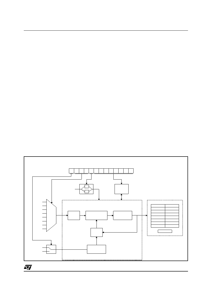
Figure 10.1 A/D Converter Structure
The pre-charging process starts by starting the
peripheral by setting to 1 the STR bit of the AD_CR
Configuration
Register.
To
speed-up
the
calibration procedure, the pre-charging phase can
be skipped when not necessary (for example when
consecutive single conversions are performed).
The user can disable the pre-charging by setting
the PRECH bit in the AD_CR Configuration
Register.
The A/D peripheral converts the input voltage with
a process of successive approximations using a
fixed clock frequency derived from the 10 MHz
internal oscillator, divided by a factor that depends
on the speed mode: about 1.6 MHz in Fast Mode
and 800 kHz in Slow Mode. The speed mode is
chosen by the SCK bit of the AD_CR Configuration
Register.
The conversion range is found between the analog
VSS and the A/D VREF references. The VREF can
be either internal, derived from the VDD, or external
by using the VREF pin. The external reference
voltage allows the application of more precise and
stable reference voltages. The two modes are
selected by using the REF bit of the AD_CR
Configuration Register.
Remark: the voltage applied to the VREF pin must
be in the range 2.7V - VDD.
The external reference voltage VREF is applied to
the analog pin PB0. This pin shares the alternate
functions with the first analog channel Ain0: if the
CONFIGURATION REGISTERS
CONTROL
LOGIC
ANALOG
MUX
Ain0
Ain1
Ain2
Ain3
Ain4
Ain5
Ain6
Ain7
VREF
VDD
AUTO-ZERO /
AUTO-CALIBRATION
COMPARATOR
SUCCESSIVE
APPROXIMATION
REGISTER
SAMPLE
&
HOLD
DAC
RESISTIVE
REFERENCE
LADDER
MSB
LSB
MSB
LSB
MSB
LSB
MSB
LSB
MSB
LSB
MSB
LSB
MSB
LSB
MSB
LSB
STATUS REGISTER
INPUT REGISTERS
VREF
SUCCESSIVE APPROXIMATION A/D CONVERTER
INT1
REF
CH0
CH1
CH2
: 6
: 12
Internal
Oscillator
10 MHz
A/D
clock
SCK
SEQ
POW
STR
CONT
INT0
RESOL
PRECH
相關(guān)PDF資料 |
PDF描述 |
|---|---|
| ST52E430B/D | 8-BIT, UVPROM, 20 MHz, MICROCONTROLLER, CDIP32 |
| ST52F510F1M6 | 8-BIT, FLASH, 24 MHz, MICROCONTROLLER, PDSO20 |
| ST52F510G0B6 | 8-BIT, FLASH, 24 MHz, MICROCONTROLLER, PDIP28 |
| ST52F513F0M6 | 8-BIT, FLASH, 24 MHz, MICROCONTROLLER, PDSO20 |
| ST52F513F1B6 | 8-BIT, FLASH, 24 MHz, MICROCONTROLLER, PDIP20 |
相關(guān)代理商/技術(shù)參數(shù) |
參數(shù)描述 |
|---|---|
| ST52510G2 | 制造商:未知廠家 制造商全稱:未知廠家 功能描述:8-BIT ICU WITH 10-BIT ADC. TWO TIMERS/PWM. I2C. SPI. SCI. UP TO 8K FLASH |
| ST52510G3 | 制造商:未知廠家 制造商全稱:未知廠家 功能描述:8-BIT ICU WITH 10-BIT ADC. TWO TIMERS/PWM. I2C. SPI. SCI. UP TO 8K FLASH |
| ST52510K2 | 制造商:未知廠家 制造商全稱:未知廠家 功能描述:8-BIT ICU WITH 10-BIT ADC. TWO TIMERS/PWM. I2C. SPI. SCI. UP TO 8K FLASH |
| ST52510K3 | 制造商:未知廠家 制造商全稱:未知廠家 功能描述:8-BIT ICU WITH 10-BIT ADC. TWO TIMERS/PWM. I2C. SPI. SCI. UP TO 8K FLASH |
| ST52510Y2 | 制造商:未知廠家 制造商全稱:未知廠家 功能描述:8-BIT ICU WITH 10-BIT ADC. TWO TIMERS/PWM. I2C. SPI. SCI. UP TO 8K FLASH |
發(fā)布緊急采購,3分鐘左右您將得到回復(fù)。