- 您現(xiàn)在的位置:買(mǎi)賣(mài)IC網(wǎng) > PDF目錄98143 > SSTUB32864EC/G (NXP SEMICONDUCTORS) 32864 SERIES, POSITIVE EDGE TRIGGERED D FLIP-FLOP, COMPLEMENTARY OUTPUT, PBGA96 PDF資料下載
參數(shù)資料
| 型號(hào): | SSTUB32864EC/G |
| 廠商: | NXP SEMICONDUCTORS |
| 元件分類(lèi): | 鎖存器 |
| 英文描述: | 32864 SERIES, POSITIVE EDGE TRIGGERED D FLIP-FLOP, COMPLEMENTARY OUTPUT, PBGA96 |
| 封裝: | 13.50 X 5.50 MM, 1.05 MM HEIGHT, LEAD FREE, PLASTIC, SOT-536-1, LFBGA-96 |
| 文件頁(yè)數(shù): | 16/19頁(yè) |
| 文件大?。?/td> | 113K |
| 代理商: | SSTUB32864EC/G |
第1頁(yè)第2頁(yè)第3頁(yè)第4頁(yè)第5頁(yè)第6頁(yè)第7頁(yè)第8頁(yè)第9頁(yè)第10頁(yè)第11頁(yè)第12頁(yè)第13頁(yè)第14頁(yè)第15頁(yè)當(dāng)前第16頁(yè)第17頁(yè)第18頁(yè)第19頁(yè)
SSTUB32864_2
NXP B.V. 2007. All rights reserved.
Product data sheet
Rev. 02 — 26 March 2007
6 of 19
NXP Semiconductors
SSTUB32864
1.8 V congurable registered buffer for DDR2-800 RDIMM applications
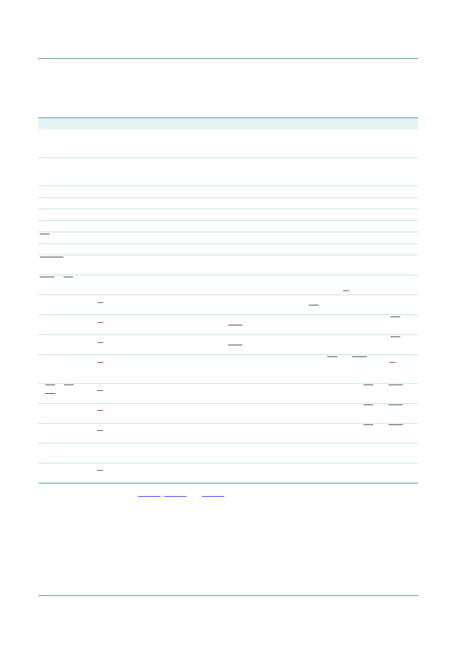
6.2 Pin description
[1]
[2]
Congurations:
Data inputs = D2, D3, D5, D6, D8 to D25 when C0 = 0 and C1 = 0.
Data inputs = D2, D3, D5, D6, D8 to D14 when C0 = 0 and C1 = 1.
Data inputs = D1 to D6, D8 to D10, D12, D13 when C0 = 1 and C1 = 1.
[3]
Congurations:
Data outputs = Q2, Q3, Q5, Q6, Q8 to Q25 when C0 = 0 and C1 = 0.
Data outputs = Q2, Q3, Q5, Q6, Q8 to Q14 when C0 = 0 and C1 = 1.
Data outputs = Q1 to Q6, Q8 to Q10, Q12, Q13 when C0 = 1 and C1 = 1.
Table 2.
Pin description
Symbol
Pin
Type
Description
GND
B3, B4, D3, D4, F3, F4,
H3, H4, K3, K4, M3,
M4, P3, P4
ground input
ground
VDD
A4, C3, C4, E3, E4,
G3, G4, J3, J4, L3, L4,
N3, N4, R3, R4, T4
1.8 V nominal
power supply voltage
VREF
A3, T3
0.9 V nominal
input reference voltage
ZOH
J5
input
reserved for future use
ZOL
J6
input
reserved for future use
CK
H1
differential input positive master clock input
CK
J1
differential input negative master clock input
C0, C1
G6, G5
LVCMOS inputs conguration control inputs
RESET
G2
LVCMOS input
Asynchronous reset input (active LOW). Resets registers and
disables VREF data and clock differential-input receivers.
CSR, DCS
J2, H2
SSTL_18 input
Chip select inputs (active LOW). Disables data outputs
switching when both inputs are HIGH.[2]
D1 to D25
SSTL_18 input
Data inputs. Clocked in on the crossing of the rising edge of
CK and the falling edge of CK.
DODT
SSTL_18 input
The outputs of this register will not be suspended by DCS and
CSR control.
DCKE
SSTL_18 input
The outputs of this register will not be suspended by DCS and
CSR control.
Q1 to Q25,
Q1A to Q14A,
Q1B to Q14B
1.8 V CMOS
outputs that are suspended by DCS and CSR control[3]
QCS, QCSA,
QCSB
1.8 V CMOS
data outputs that will not be suspended by DCS and CSR
control
QODT, QODTA,
QODTB
1.8 V CMOS
data outputs that will not be suspended by DCS and CSR
control
QCKE, QCKEA,
QCKEB
1.8 V CMOS
data outputs that will not be suspended by DCS and CSR
control
n.c.
A2, D2, G1
-
Not connected. Ball present but no internal connection to the
die.
DNU
-
Do-not-use. Ball internally connected to the die which should
be left open-circuit.
相關(guān)PDF資料 |
PDF描述 |
|---|---|
| SSTUB32868ET/S | 32868 SERIES, POSITIVE EDGE TRIGGERED D FLIP-FLOP, TRUE OUTPUT, PBGA176 |
| SSTUG32865ET/S | SSTU SERIES, POSITIVE EDGE TRIGGERED D FLIP-FLOP, TRUE OUTPUT, PBGA160 |
| SSTUG32868ET/G | 32868 SERIES, POSITIVE EDGE TRIGGERED D FLIP-FLOP, COMPLEMENTARY OUTPUT, PBGA176 |
| SSTUP32866EC/S | 32866 SERIES, POSITIVE EDGE TRIGGERED D FLIP-FLOP, COMPLEMENTARY OUTPUT, PBGA96 |
| SSTV16857EC | POSITIVE EDGE TRIGGERED D FLIP-FLOP, TRUE OUTPUT, PBGA56 |
相關(guān)代理商/技術(shù)參數(shù) |
參數(shù)描述 |
|---|---|
| SSTUB32865 | 制造商:PHILIPS 制造商全稱(chēng):NXP Semiconductors 功能描述:1.8 V 28-bit 1 : 2 registered buffer with parity for DDR2-800 RDIMM applications |
| SSTUB32865ET/G,518 | 功能描述:寄存器 1.8V 28B REG RoHS:否 制造商:NXP Semiconductors 邏輯類(lèi)型:CMOS 邏輯系列:HC 電路數(shù)量:1 最大時(shí)鐘頻率:36 MHz 傳播延遲時(shí)間: 高電平輸出電流:- 7.8 mA 低電平輸出電流:7.8 mA 電源電壓-最大:6 V 最大工作溫度:+ 125 C 封裝 / 箱體:SOT-38 封裝:Tube |
| SSTUB32865ET/G-T | 功能描述:寄存器 1.8V 28B REG BUF/PRTY DDR2-800 RoHS:否 制造商:NXP Semiconductors 邏輯類(lèi)型:CMOS 邏輯系列:HC 電路數(shù)量:1 最大時(shí)鐘頻率:36 MHz 傳播延遲時(shí)間: 高電平輸出電流:- 7.8 mA 低電平輸出電流:7.8 mA 電源電壓-最大:6 V 最大工作溫度:+ 125 C 封裝 / 箱體:SOT-38 封裝:Tube |
| SSTUB32866 | 制造商:PHILIPS 制造商全稱(chēng):NXP Semiconductors 功能描述:1.8 V 25-bit 1 : 1 or 14-bit 1 : 2 configurable registered buffer with parity for DDR2-800 RDIMM applications |
| SSTUB32866_10 | 制造商:PHILIPS 制造商全稱(chēng):NXP Semiconductors 功能描述:1.8 V 25-bit 1 : 1 or 14-bit 1 : 2 configurable registered buffer with parity for DDR2-800 RDIMM applications |
發(fā)布緊急采購(gòu),3分鐘左右您將得到回復(fù)。