- 您現(xiàn)在的位置:買賣IC網(wǎng) > PDF目錄374843 > SMJ55161 (Texas Instruments, Inc.) 262144 BY 16-BIT MULTIPORT VIDEO RAM PDF資料下載
參數(shù)資料
| 型號: | SMJ55161 |
| 廠商: | Texas Instruments, Inc. |
| 英文描述: | 262144 BY 16-BIT MULTIPORT VIDEO RAM |
| 中文描述: | 262144由16位多端口視頻內(nèi)存 |
| 文件頁數(shù): | 1/64頁 |
| 文件大小: | 1505K |
| 代理商: | SMJ55161 |
當(dāng)前第1頁第2頁第3頁第4頁第5頁第6頁第7頁第8頁第9頁第10頁第11頁第12頁第13頁第14頁第15頁第16頁第17頁第18頁第19頁第20頁第21頁第22頁第23頁第24頁第25頁第26頁第27頁第28頁第29頁第30頁第31頁第32頁第33頁第34頁第35頁第36頁第37頁第38頁第39頁第40頁第41頁第42頁第43頁第44頁第45頁第46頁第47頁第48頁第49頁第50頁第51頁第52頁第53頁第54頁第55頁第56頁第57頁第58頁第59頁第60頁第61頁第62頁第63頁第64頁
ta(R)
(MAX)
75 ns
ta(SQ)
(MAX)
23 ns
tc(W)
(MIN)
140 ns
SMJ55161-75
SMJ55161-80
80 ns
25 ns
150 ns
tc(P)
(MIN)
48 ns
tc(SC)
(MIN)
24 ns
ICC1
(MAX)
165 mA
ICC1A
(MAX)
210 mA
50 ns
30 ns
160 mA
195 mA
ROW ENABLE
SERIAL DATA
CYCLE TIME
PAGE MODE
CYCLE TIME
SERIAL PORT STAND-
BY
SERIAL PORT AC-
TIVE
ACCESS TIME
ACCESS TIME
DRAM
DRAM
SERIAL
OPERATING CURRENT
OPERATING CURRENT
SMJ55161
262144 BY 16-BIT
MULTIPORT VIDEO RAM
SGMS056D – MAY 1995 – REVISED OCTOBER 1997
1
POST OFFICE BOX 1443
HOUSTON, TEXAS 77251–1443
Organization:
– DRAM: 262 144 by 16 Bits
– SAM: 256 by 16 Bits
Dual-Port Accessibility – Simultaneous and
Asynchronous Access From the DRAM and
SAM Ports
Data-Transfer Function From the DRAM to
the Serial-Data Register
(4
×
4)
×
4 Block-Write Feature for Fast
Area-Fill Operations; as Many as Four
Memory-Address Locations Written Per
Cycle From the 16-Bit On-Chip Color
Register
Write-Per-Bit Feature for Selective Write to
Each RAM I/O; Two Write-Per-Bit Modes to
Simplify System Design
Byte-Write Control (CASL, CASU) Provides
Flexibility
Extended Data Output for Faster System
Cycle Time
Enhanced Page-Mode Operation for Faster
Access
CAS-Before-RAS (CBR) and
Hidden-Refresh Modes
Long Refresh Period
Every 8 ms (Maximum)
Up to 45-MHz Uninterrupted Serial-Data
Streams
256 Selectable Serial-Register Starting
Locations
SE-Controlled Register-Status QSF
Split-Register-Transfer Read for Simplified
Real-Time Register Load
Performance Ranges:
Programmable Split-Register Stop Point
3-State Serial Outputs Allow Easy
Multiplexing of Video-Data Streams
All Inputs/Outputs and Clocks TTL
Compatible
Compatible With JEDEC Standards
Designed to Work With the Texas
Instruments Graphics Family
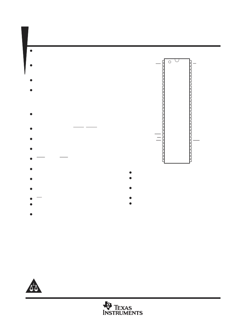
TRG
VSS
SQ0
DQ0
SQ1
DQ1
VCC
SQ2
DQ2
SQ3
DQ3
VSS
SQ4
DQ4
SQ5
DQ5
VCC
SQ6
DQ6
SQ7
DQ7
VSS
CASL
WE
RAS
SC
SE
VSS
SQ15
DQ15
SQ14
DQ14
VCC
SQ13
DQ13
SQ12
DQ12
VSS
SQ11
DQ11
SQ10
DQ10
VCC
SQ9
DQ9
SQ8
DQ8
VSS
DSF
NC / GND
CASU
QSF
A0
A1
A2
A3
VSS
VCC
A8
A7
A6
A5
A4
VCC
1
2
3
4
5
6
7
8
9
10
11
12
13
14
15
16
17
18
19
20
21
22
23
24
25
26
27
28
29
30
31
32
64
63
62
61
60
59
58
57
56
55
54
53
52
51
50
49
48
47
46
45
44
43
42
41
40
39
38
37
36
35
34
33
HKC PACKAGE
(TOP VIEW)
PRODUCTION DATA information is current as of publication date.
Products conform to specifications per the terms of Texas Instruments
standard warranty. Production processing does not necessarily include
testing of all parameters.
Copyright
1997, Texas Instruments Incorporated
Please be aware that an important notice concerning availability, standard warranty, and use in critical applications of
Texas Instruments semiconductor products and disclaimers thereto appears at the end of this data sheet.
相關(guān)PDF資料 |
PDF描述 |
|---|---|
| SMJ55166 | 262144 BY 16-BIT MULTIPORT VIDEO RAM |
| SMJ626162 | 524288 BY 16-BIT BY 2-BANK SYNCHRONOUS DYNAMIC RANDOM-ACCESS MEMORY |
| SML-010DT | Chip LEDs with reflectors |
| SML-010FT | Chip LEDs with reflectors |
| SML-010JT | Chip LEDs with reflectors |
相關(guān)代理商/技術(shù)參數(shù) |
參數(shù)描述 |
|---|---|
| SMJ55166 | 制造商:TI 制造商全稱:Texas Instruments 功能描述:262144 BY 16-BIT MULTIPORT VIDEO RAM |
| SMJ55166-75HKCM | 制造商:Micross Components 功能描述:DRAM 2KX16 "VIDEO RAM" - Bulk |
| SMJ5821TS50 | 制造商:MICRO SEMI 功能描述:New |
| SMJ5C1008-25JDCM | 制造商:Rochester Electronics LLC 功能描述:- Bulk |
| SMJ5C1008L-25JDCM | 制造商:Texas Instruments 功能描述: |
發(fā)布緊急采購,3分鐘左右您將得到回復(fù)。