- 您現(xiàn)在的位置:買賣IC網(wǎng) > PDF目錄383724 > ORT8850L Field-Programmable System Chip (FPSC) Eight-Channel x 850 Mbits/s Backplane Transceiver PDF資料下載
參數(shù)資料
| 型號: | ORT8850L |
| 英文描述: | Field-Programmable System Chip (FPSC) Eight-Channel x 850 Mbits/s Backplane Transceiver |
| 中文描述: | 現(xiàn)場可編程系統(tǒng)芯片(促進文化基金)8通道x 850 Mbits /秒背板收發(fā)器 |
| 文件頁數(shù): | 55/112頁 |
| 文件大小: | 2417K |
| 代理商: | ORT8850L |
第1頁第2頁第3頁第4頁第5頁第6頁第7頁第8頁第9頁第10頁第11頁第12頁第13頁第14頁第15頁第16頁第17頁第18頁第19頁第20頁第21頁第22頁第23頁第24頁第25頁第26頁第27頁第28頁第29頁第30頁第31頁第32頁第33頁第34頁第35頁第36頁第37頁第38頁第39頁第40頁第41頁第42頁第43頁第44頁第45頁第46頁第47頁第48頁第49頁第50頁第51頁第52頁第53頁第54頁當前第55頁第56頁第57頁第58頁第59頁第60頁第61頁第62頁第63頁第64頁第65頁第66頁第67頁第68頁第69頁第70頁第71頁第72頁第73頁第74頁第75頁第76頁第77頁第78頁第79頁第80頁第81頁第82頁第83頁第84頁第85頁第86頁第87頁第88頁第89頁第90頁第91頁第92頁第93頁第94頁第95頁第96頁第97頁第98頁第99頁第100頁第101頁第102頁第103頁第104頁第105頁第106頁第107頁第108頁第109頁第110頁第111頁第112頁
Agere Systems Inc.
55
Data Sheet
August 2001
Eight-Channel x 850 Mbits/s Backplane Transceiver
ORCA
ORT8850 FPSC
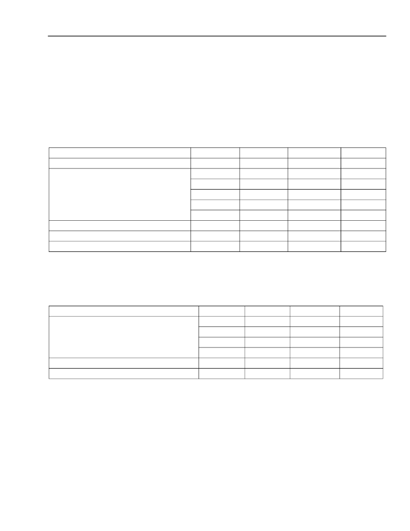
Absolute Maximum Ratings
Stresses in excess of the absolute maximum ratings can cause permanent damage to the device. These are abso-
lute stress ratings only. Functional operation of the device is not implied at these or any other conditions in excess
of those given in the operations sections of this data sheet. Exposure to absolute maximum ratings for extended
periods can adversely affect device reliability.
The
ORCA
Series 3+ FPSCs include circuitry designed to protect the chips from damaging substrate injection cur-
rents and to prevent accumulations of static charge. Nevertheless, conventional precautions should be observed
during storage, handling, and use to avoid exposure to excessive electrical stress.
Table 13. Absolute Maximum Ratings
* V
DD
A_SHIM and V
DD
A_STM are analog power supply inputs which need to be isolated from other power supplies on the board.
Recommended Operating Conditions
Table 14. Recommended Operating Conditions
* For recommended operating conditions for V
DD
IO, see the
Series 4 FPGA Data Sheet
and the
Series 4 I/O Buffer Application Note
.
V
DD
A_SHIM and V
DD
A_STM are analog power supply inputs which need to be isolated from other power supplies on the board.
V
DD
33 is an analog power supply for the FPGA PLLs and needs to be isolated from other power supplies on the board.
Parameter
Symbol
T
stg
V
DD
33
V
DD
IO
V
DD
15
V
DD
A_SHIM*
V
DD
A_STM*
—
—
—
Min
–
65
–
0.3
–
0.3
–
0.3
–
0.3
–
0.3
–
0.3
–
0.3
—
Max
150
4.2
4.2
2.0
2.0
2.0
Unit
°
C
V
V
V
V
V
V
V
°
C
Storage Temperature
Power Supply Voltage with Respect to Ground
Input Signal with Respect to Ground
Signal Applied to High-impedance Output
Maximum Package Body Temperature
V
DDIO
+ 0.3
V
DDIO
+ 0.3
220
Parameter
Symbol
V
DD
33
V
DD
15
V
DD
A_SHIM
V
DD
A_STM
V
IN
T
J
Min
2.7
1.4
1.4
1.4
–
0.3
–
40
Max
3.6
1.6
1.6
1.6
Unit
V
V
V
V
V
°
C
Power Supply Voltage with Respect to Ground*
Input Voltages
Junction Temperature
V
DDIO
+ 0.3
125
相關(guān)PDF資料 |
PDF描述 |
|---|---|
| OS1001 | Interface IC |
| OS1010 | Optoelectronic |
| OS1011 | SINGLE 1.8V, 200 KHZ OP, E TEMP, -40C to +125C, 8-PDIP, TUBE |
| OS1012 | 1.8V, 200kHz single low-cost, CMOS Op Amplifier on 120K Analog ROM process., -40C to +125C, 8-MSOP, T/R |
| OS1013 | 1.8V, 200kHz single low-cost, CMOS Op Amplifier on 120K Analog ROM proccess., -40C to +125C, 5-SOT-23, T/R |
相關(guān)代理商/技術(shù)參數(shù) |
參數(shù)描述 |
|---|---|
| ORT8850L-1BM680C | 功能描述:FPGA - 現(xiàn)場可編程門陣列 4992 LUT 278 I/O RoHS:否 制造商:Altera Corporation 系列:Cyclone V E 柵極數(shù)量: 邏輯塊數(shù)量:943 內(nèi)嵌式塊RAM - EBR:1956 kbit 輸入/輸出端數(shù)量:128 最大工作頻率:800 MHz 工作電源電壓:1.1 V 最大工作溫度:+ 70 C 安裝風格:SMD/SMT 封裝 / 箱體:FBGA-256 |
| ORT8850L-1BM680I | 功能描述:FPGA - 現(xiàn)場可編程門陣列 4992 LUT 278 I/O RoHS:否 制造商:Altera Corporation 系列:Cyclone V E 柵極數(shù)量: 邏輯塊數(shù)量:943 內(nèi)嵌式塊RAM - EBR:1956 kbit 輸入/輸出端數(shù)量:128 最大工作頻率:800 MHz 工作電源電壓:1.1 V 最大工作溫度:+ 70 C 安裝風格:SMD/SMT 封裝 / 箱體:FBGA-256 |
| ORT8850L-1BMN680C | 功能描述:FPGA - 現(xiàn)場可編程門陣列 4992 LUT 278 I/O RoHS:否 制造商:Altera Corporation 系列:Cyclone V E 柵極數(shù)量: 邏輯塊數(shù)量:943 內(nèi)嵌式塊RAM - EBR:1956 kbit 輸入/輸出端數(shù)量:128 最大工作頻率:800 MHz 工作電源電壓:1.1 V 最大工作溫度:+ 70 C 安裝風格:SMD/SMT 封裝 / 箱體:FBGA-256 |
| ORT8850L-1BMN680I | 功能描述:FPGA - 現(xiàn)場可編程門陣列 4992 LUT 278 I/O RoHS:否 制造商:Altera Corporation 系列:Cyclone V E 柵極數(shù)量: 邏輯塊數(shù)量:943 內(nèi)嵌式塊RAM - EBR:1956 kbit 輸入/輸出端數(shù)量:128 最大工作頻率:800 MHz 工作電源電壓:1.1 V 最大工作溫度:+ 70 C 安裝風格:SMD/SMT 封裝 / 箱體:FBGA-256 |
| ORT8850L-2BM680C | 功能描述:FPGA - 現(xiàn)場可編程門陣列 4992 LUT 278 I/O RoHS:否 制造商:Altera Corporation 系列:Cyclone V E 柵極數(shù)量: 邏輯塊數(shù)量:943 內(nèi)嵌式塊RAM - EBR:1956 kbit 輸入/輸出端數(shù)量:128 最大工作頻率:800 MHz 工作電源電壓:1.1 V 最大工作溫度:+ 70 C 安裝風格:SMD/SMT 封裝 / 箱體:FBGA-256 |
發(fā)布緊急采購,3分鐘左右您將得到回復。