- 您現(xiàn)在的位置:買賣IC網(wǎng) > PDF目錄383724 > ORT8850L Field-Programmable System Chip (FPSC) Eight-Channel x 850 Mbits/s Backplane Transceiver PDF資料下載
參數(shù)資料
| 型號(hào): | ORT8850L |
| 英文描述: | Field-Programmable System Chip (FPSC) Eight-Channel x 850 Mbits/s Backplane Transceiver |
| 中文描述: | 現(xiàn)場(chǎng)可編程系統(tǒng)芯片(促進(jìn)文化基金)8通道x 850 Mbits /秒背板收發(fā)器 |
| 文件頁(yè)數(shù): | 40/112頁(yè) |
| 文件大?。?/td> | 2417K |
| 代理商: | ORT8850L |
第1頁(yè)第2頁(yè)第3頁(yè)第4頁(yè)第5頁(yè)第6頁(yè)第7頁(yè)第8頁(yè)第9頁(yè)第10頁(yè)第11頁(yè)第12頁(yè)第13頁(yè)第14頁(yè)第15頁(yè)第16頁(yè)第17頁(yè)第18頁(yè)第19頁(yè)第20頁(yè)第21頁(yè)第22頁(yè)第23頁(yè)第24頁(yè)第25頁(yè)第26頁(yè)第27頁(yè)第28頁(yè)第29頁(yè)第30頁(yè)第31頁(yè)第32頁(yè)第33頁(yè)第34頁(yè)第35頁(yè)第36頁(yè)第37頁(yè)第38頁(yè)第39頁(yè)當(dāng)前第40頁(yè)第41頁(yè)第42頁(yè)第43頁(yè)第44頁(yè)第45頁(yè)第46頁(yè)第47頁(yè)第48頁(yè)第49頁(yè)第50頁(yè)第51頁(yè)第52頁(yè)第53頁(yè)第54頁(yè)第55頁(yè)第56頁(yè)第57頁(yè)第58頁(yè)第59頁(yè)第60頁(yè)第61頁(yè)第62頁(yè)第63頁(yè)第64頁(yè)第65頁(yè)第66頁(yè)第67頁(yè)第68頁(yè)第69頁(yè)第70頁(yè)第71頁(yè)第72頁(yè)第73頁(yè)第74頁(yè)第75頁(yè)第76頁(yè)第77頁(yè)第78頁(yè)第79頁(yè)第80頁(yè)第81頁(yè)第82頁(yè)第83頁(yè)第84頁(yè)第85頁(yè)第86頁(yè)第87頁(yè)第88頁(yè)第89頁(yè)第90頁(yè)第91頁(yè)第92頁(yè)第93頁(yè)第94頁(yè)第95頁(yè)第96頁(yè)第97頁(yè)第98頁(yè)第99頁(yè)第100頁(yè)第101頁(yè)第102頁(yè)第103頁(yè)第104頁(yè)第105頁(yè)第106頁(yè)第107頁(yè)第108頁(yè)第109頁(yè)第110頁(yè)第111頁(yè)第112頁(yè)
40
Agere Systems Inc.
Data Sheet
August 2001
Eight-Channel x 850 Mbits/s Backplane Transceiver
ORCA
ORT8850 FPSC
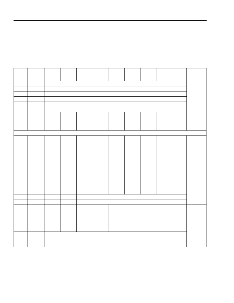
Memory Map
(continued)
This table is constructed to show the correct values when read and written via the system bus MPI interface. When
using this table while interfacing with the system bus user logic master interface, the data values will need to be
byte flipped. This is due to the opposite orientation of the MPI and master interface bus ordering. More information
on this can be found in the MPI/System Bus Application Note (AP01-032NCIP).
Table 11. Memory Map
(This table resides at memory offset 0X30000 in the ORT8850.)
ADDR
[7:0]
Register
Type
DB7
DB6
DB5
DB4
DB3
DB2
DB1
DB0
MSB
Reset
Value
[7:0]
Comment
00
01
02
03
04
05
06
sreg
sreg
sreg
creg
creg
creg
preg
fixed rev [0:7]
fixed id lsb [0:7]
fixed id msb [0:7]
scratch pad [0:7]
lockreg msb [0:7]
lockreg lsb [0:7]
—
05
80
80
00
00
00
NA
g
—
—
—
—
—
—
global
reset
comman
d
Device Register Block
08
creg
—
—
—
“
rx toh
frame
”
and
“
rx
toh clk
enable
”
hiz
control
serial port
output
MUX
select for
ch#5
ext prot
sw en
—
—
lvds lpbk
control
(CDR
only)
00
d
09
creg
parallel
port
output
MUX
select for
ch#7
—
—
—
parallel
port
output
MUX
select for
ch#5
—
—
serial
port
output
MUX
select for
ch#7
—
—
parallel
port
output
MUX
select for
ch#3
FIFO aligner threshold value (min) [0:4]
FIFO aligner threshold value (max) [0:4]
line lpbk
control
parallel
port
output
MUX
select for
ch#1
serial
port
output
MUX
select for
ch#3
serial
port
output
MUX
select for
ch#1
FF
(4 ch
was 0F)
0a
0b
0c
creg
creg
creg
40
A8
06
scram-
bler/
descra-
mbler
control
input/
output
parallel
bus
parity
control
number of consecutive A1 A2 errors to
generate [0:3]
d
0d
0e
0f
creg
creg
creg
a1 error insert value [0:7]
a2 error insert value [0:7]
transmitter B1 error insert mask [0:7]
00
00
00
相關(guān)PDF資料 |
PDF描述 |
|---|---|
| OS1001 | Interface IC |
| OS1010 | Optoelectronic |
| OS1011 | SINGLE 1.8V, 200 KHZ OP, E TEMP, -40C to +125C, 8-PDIP, TUBE |
| OS1012 | 1.8V, 200kHz single low-cost, CMOS Op Amplifier on 120K Analog ROM process., -40C to +125C, 8-MSOP, T/R |
| OS1013 | 1.8V, 200kHz single low-cost, CMOS Op Amplifier on 120K Analog ROM proccess., -40C to +125C, 5-SOT-23, T/R |
相關(guān)代理商/技術(shù)參數(shù) |
參數(shù)描述 |
|---|---|
| ORT8850L-1BM680C | 功能描述:FPGA - 現(xiàn)場(chǎng)可編程門陣列 4992 LUT 278 I/O RoHS:否 制造商:Altera Corporation 系列:Cyclone V E 柵極數(shù)量: 邏輯塊數(shù)量:943 內(nèi)嵌式塊RAM - EBR:1956 kbit 輸入/輸出端數(shù)量:128 最大工作頻率:800 MHz 工作電源電壓:1.1 V 最大工作溫度:+ 70 C 安裝風(fēng)格:SMD/SMT 封裝 / 箱體:FBGA-256 |
| ORT8850L-1BM680I | 功能描述:FPGA - 現(xiàn)場(chǎng)可編程門陣列 4992 LUT 278 I/O RoHS:否 制造商:Altera Corporation 系列:Cyclone V E 柵極數(shù)量: 邏輯塊數(shù)量:943 內(nèi)嵌式塊RAM - EBR:1956 kbit 輸入/輸出端數(shù)量:128 最大工作頻率:800 MHz 工作電源電壓:1.1 V 最大工作溫度:+ 70 C 安裝風(fēng)格:SMD/SMT 封裝 / 箱體:FBGA-256 |
| ORT8850L-1BMN680C | 功能描述:FPGA - 現(xiàn)場(chǎng)可編程門陣列 4992 LUT 278 I/O RoHS:否 制造商:Altera Corporation 系列:Cyclone V E 柵極數(shù)量: 邏輯塊數(shù)量:943 內(nèi)嵌式塊RAM - EBR:1956 kbit 輸入/輸出端數(shù)量:128 最大工作頻率:800 MHz 工作電源電壓:1.1 V 最大工作溫度:+ 70 C 安裝風(fēng)格:SMD/SMT 封裝 / 箱體:FBGA-256 |
| ORT8850L-1BMN680I | 功能描述:FPGA - 現(xiàn)場(chǎng)可編程門陣列 4992 LUT 278 I/O RoHS:否 制造商:Altera Corporation 系列:Cyclone V E 柵極數(shù)量: 邏輯塊數(shù)量:943 內(nèi)嵌式塊RAM - EBR:1956 kbit 輸入/輸出端數(shù)量:128 最大工作頻率:800 MHz 工作電源電壓:1.1 V 最大工作溫度:+ 70 C 安裝風(fēng)格:SMD/SMT 封裝 / 箱體:FBGA-256 |
| ORT8850L-2BM680C | 功能描述:FPGA - 現(xiàn)場(chǎng)可編程門陣列 4992 LUT 278 I/O RoHS:否 制造商:Altera Corporation 系列:Cyclone V E 柵極數(shù)量: 邏輯塊數(shù)量:943 內(nèi)嵌式塊RAM - EBR:1956 kbit 輸入/輸出端數(shù)量:128 最大工作頻率:800 MHz 工作電源電壓:1.1 V 最大工作溫度:+ 70 C 安裝風(fēng)格:SMD/SMT 封裝 / 箱體:FBGA-256 |
發(fā)布緊急采購(gòu),3分鐘左右您將得到回復(fù)。