- 您現(xiàn)在的位置:買賣IC網(wǎng) > PDF目錄1958 > ORSO82G5-3F680C (Lattice Semiconductor Corporation)IC FPSC TRANSCEIVER 8CH 680-BGA PDF資料下載
參數(shù)資料
| 型號(hào): | ORSO82G5-3F680C |
| 廠商: | Lattice Semiconductor Corporation |
| 文件頁數(shù): | 109/153頁 |
| 文件大小: | 0K |
| 描述: | IC FPSC TRANSCEIVER 8CH 680-BGA |
| 產(chǎn)品變化通告: | Product Discontinuation 01/Aug/2011 |
| 標(biāo)準(zhǔn)包裝: | 24 |
| 系列: | * |
第1頁第2頁第3頁第4頁第5頁第6頁第7頁第8頁第9頁第10頁第11頁第12頁第13頁第14頁第15頁第16頁第17頁第18頁第19頁第20頁第21頁第22頁第23頁第24頁第25頁第26頁第27頁第28頁第29頁第30頁第31頁第32頁第33頁第34頁第35頁第36頁第37頁第38頁第39頁第40頁第41頁第42頁第43頁第44頁第45頁第46頁第47頁第48頁第49頁第50頁第51頁第52頁第53頁第54頁第55頁第56頁第57頁第58頁第59頁第60頁第61頁第62頁第63頁第64頁第65頁第66頁第67頁第68頁第69頁第70頁第71頁第72頁第73頁第74頁第75頁第76頁第77頁第78頁第79頁第80頁第81頁第82頁第83頁第84頁第85頁第86頁第87頁第88頁第89頁第90頁第91頁第92頁第93頁第94頁第95頁第96頁第97頁第98頁第99頁第100頁第101頁第102頁第103頁第104頁第105頁第106頁第107頁第108頁當(dāng)前第109頁第110頁第111頁第112頁第113頁第114頁第115頁第116頁第117頁第118頁第119頁第120頁第121頁第122頁第123頁第124頁第125頁第126頁第127頁第128頁第129頁第130頁第131頁第132頁第133頁第134頁第135頁第136頁第137頁第138頁第139頁第140頁第141頁第142頁第143頁第144頁第145頁第146頁第147頁第148頁第149頁第150頁第151頁第152頁第153頁
Lattice Semiconductor
ORCA ORSO42G5 and ORSO82G5 Data Sheet
59
The behavior of the IPC is dependent on the AUTO_BUNDLE register bit. If AUTO_BUNDLE is set, the group will
continue to operate even if a link (or several links) of the group is not valid (RX_LINK_GOOD is low). If
AUTO_BUNDLE is not set the entire group must be valid (RX_LINK_GOOD is high) for the group to receive cells
through the IPC.
The IPC must determine when FIFO reads may begin. Before reading data from a FIFO can begin, the FIFO must
have a full cell available to be read. This is condition is indicated by a signal from each FIFO which is monitored by
the IPC. The IPC then makes sure that the cells in a given port are received in the order that they are transmitted.
IPC Receive Cell Mode Timing Core/FPGA
This section contains timing diagrams for major interfaces of this block to the FPGA logic when cells are to be
transferred. Figure 45 shows the cell twin-link mode timing. The number of clock cycles to transfer the cell data
depends on the payload size selected. Error indications for CELL BIP errors and CELL DROP are also shown.
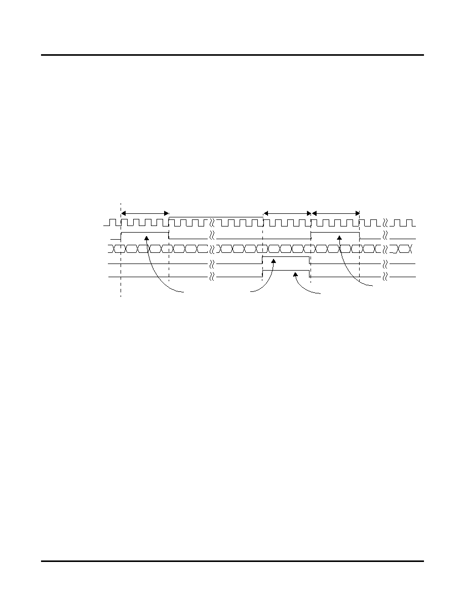
Figure 45. IPC2 Data Flow
When operating in CELL MODE, the IPC2 Block passes user cells as well as control and status signals to the user.
Depending upon the congured CELL SIZE, cell transfers will take a variable number of SYSCLK156 cycles to be
received across the interface. Data are always transferred across a 40-bit bus (5 octets per clock cycle). Figure 45
shows 16 clock cycles for a cell transfer. This corresponds to a User Cell size of 79 octets.
Figure 46 shows cell octal alignment mode timing for the ORSO82G5. When operating in CELL MODE, the IPC8
Block aligns all 8 channels of receive data on a FRAME basis. The IPC8 also passes user cells as well as control
and status signals to the user. Depending upon the congured CELL SIZE, cell transfers will take a variable num-
ber of SYSCLK156 cycles to be received across the interface. Data are always transferred across an 160-bit bus
(20 octets per clock cycle). Figure 46 shows 4 clock cycles for a cell transfer. This corresponds to a User Cell size
of 79 octets.
SYSCLK156x[1,2]
IPC2_A[1,2]CELLSTART
D
DD
D
DD
D
DD
D
DDDD
4 clk cycles
“n” clk cycles
4 clk cycles
CELL BIP ERROR
If a Cell BIP Error occurs,
the CELL_BIP_ERR signal reects the occurrence, as shown in the
Figure.
For 2-Link CELL MODE,
the CELL_BIP_ERR signal is asserted during the last 4 clock cycles
of the receive cell.
4 clk cycles
D
IPC2_A[1,2]_BIP_ERR
IPC2_A[1,2]_CELLDROP
IPC2_x[1,2][39:0]
BIP Error is associated
with CURRENT cell
Cell Drop is associated with
the NEXT cell (NOT present)
CELL BIP ERROR
If a cell error occurs within the ASB and;
1. CELL_BIP_INH=0 ...Do not drop BIP errored cells
(s/w selectable)
2. A BIP error occurs
The drop indicator will PRECEED the user cell that con-
tains the BIP error. All data will be passed w/o modica-
tion.
相關(guān)PDF資料 |
PDF描述 |
|---|---|
| ORT82G5-3F680C | IC FPSC TRANSCEIVER 8CH 680-BGA |
| ORT8850L-1BMN680I | IC TRANCEIVERS FPSC 680FPGAM |
| ORT8850L-3BM680C | IC FPSC TRANSCEIVER 8CH 680-BGA |
| P1010PSE5HFA | MPU PROTO 800/667 425-TEPBGA1 |
| P1013NXN2LFB | IC MPU 1067MHZ 689TEPBGA |
相關(guān)代理商/技術(shù)參數(shù) |
參數(shù)描述 |
|---|---|
| ORSO82G5-3FN680C | 功能描述:FPGA - 現(xiàn)場可編程門陣列 ORCA FPSC 1.5V 2.7 G b Bpln Xcvr 643K Gt RoHS:否 制造商:Altera Corporation 系列:Cyclone V E 柵極數(shù)量: 邏輯塊數(shù)量:943 內(nèi)嵌式塊RAM - EBR:1956 kbit 輸入/輸出端數(shù)量:128 最大工作頻率:800 MHz 工作電源電壓:1.1 V 最大工作溫度:+ 70 C 安裝風(fēng)格:SMD/SMT 封裝 / 箱體:FBGA-256 |
| ORSO82G5-3FN680C1 | 功能描述:FPGA - 現(xiàn)場可編程門陣列 10368 LUT 372 I/O RoHS:否 制造商:Altera Corporation 系列:Cyclone V E 柵極數(shù)量: 邏輯塊數(shù)量:943 內(nèi)嵌式塊RAM - EBR:1956 kbit 輸入/輸出端數(shù)量:128 最大工作頻率:800 MHz 工作電源電壓:1.1 V 最大工作溫度:+ 70 C 安裝風(fēng)格:SMD/SMT 封裝 / 箱體:FBGA-256 |
| ORSO82G5-G2-PAC-EV | 功能描述:可編程邏輯 IC 開發(fā)工具 ORCA ORSO82G5-FPSC Eval Brd RoHS:否 制造商:Altera Corporation 產(chǎn)品:Development Kits 類型:FPGA 工具用于評(píng)估:5CEFA7F3 接口類型: 工作電源電壓: |
| ORSPI4 | 制造商:LATTICE 制造商全稱:Lattice Semiconductor 功能描述:Dual SPI4 Interface and High-Speed SERDES FPSC |
| ORSPI4-1F1156C | 功能描述:FPGA - 現(xiàn)場可編程門陣列 16192 LUT RoHS:否 制造商:Altera Corporation 系列:Cyclone V E 柵極數(shù)量: 邏輯塊數(shù)量:943 內(nèi)嵌式塊RAM - EBR:1956 kbit 輸入/輸出端數(shù)量:128 最大工作頻率:800 MHz 工作電源電壓:1.1 V 最大工作溫度:+ 70 C 安裝風(fēng)格:SMD/SMT 封裝 / 箱體:FBGA-256 |
發(fā)布緊急采購,3分鐘左右您將得到回復(fù)。