- 您現(xiàn)在的位置:買賣IC網 > PDF目錄383723 > OR3TP12-6BA352 Quad 2.3V 10 MHz OP, I temp, -40C to +85C, 14-PDIP, TUBE PDF資料下載
參數資料
| 型號: | OR3TP12-6BA352 |
| 英文描述: | Quad 2.3V 10 MHz OP, I temp, -40C to +85C, 14-PDIP, TUBE |
| 中文描述: | 用戶可編程ASIC的特殊功能 |
| 文件頁數: | 59/128頁 |
| 文件大小: | 2450K |
| 代理商: | OR3TP12-6BA352 |
第1頁第2頁第3頁第4頁第5頁第6頁第7頁第8頁第9頁第10頁第11頁第12頁第13頁第14頁第15頁第16頁第17頁第18頁第19頁第20頁第21頁第22頁第23頁第24頁第25頁第26頁第27頁第28頁第29頁第30頁第31頁第32頁第33頁第34頁第35頁第36頁第37頁第38頁第39頁第40頁第41頁第42頁第43頁第44頁第45頁第46頁第47頁第48頁第49頁第50頁第51頁第52頁第53頁第54頁第55頁第56頁第57頁第58頁當前第59頁第60頁第61頁第62頁第63頁第64頁第65頁第66頁第67頁第68頁第69頁第70頁第71頁第72頁第73頁第74頁第75頁第76頁第77頁第78頁第79頁第80頁第81頁第82頁第83頁第84頁第85頁第86頁第87頁第88頁第89頁第90頁第91頁第92頁第93頁第94頁第95頁第96頁第97頁第98頁第99頁第100頁第101頁第102頁第103頁第104頁第105頁第106頁第107頁第108頁第109頁第110頁第111頁第112頁第113頁第114頁第115頁第116頁第117頁第118頁第119頁第120頁第121頁第122頁第123頁第124頁第125頁第126頁第127頁第128頁
Lucent Technologies Inc.
Lucent Technologies Inc.
59
Data Sheet
March 2000
ORCA OR3TP12 FPSC
Embedded Master/Target PCI Interface
PCI Bus Core Target Controller Detailed Description
(continued)
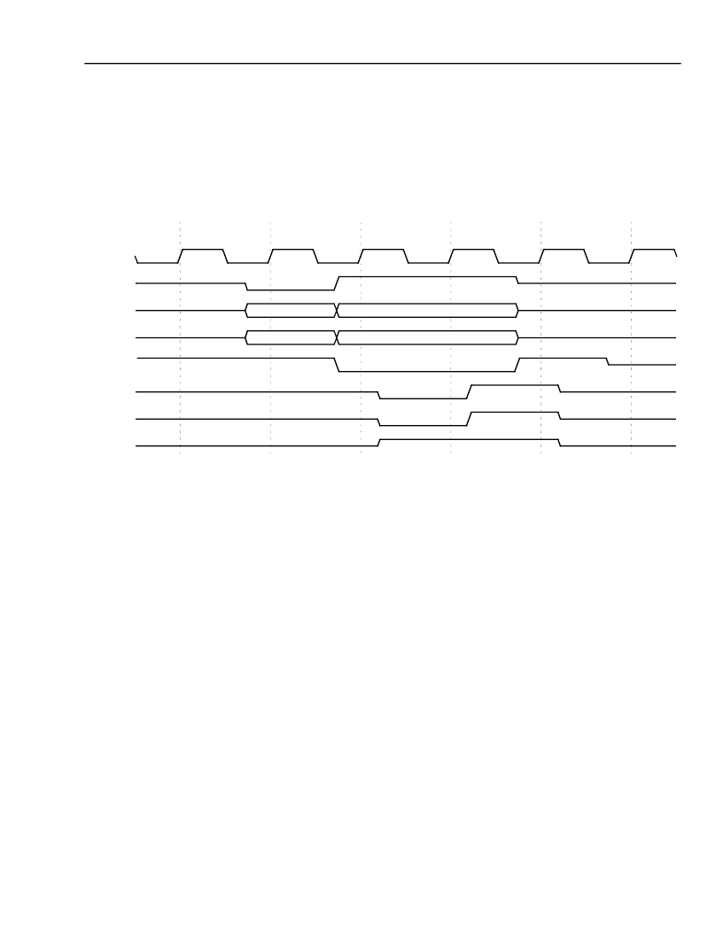
Target Write Memory, Single-Word Transaction
Figure 17 shows the timing on the PCI bus, for a Target memory write of a single word. The timing on the PCI inter-
face (Figure 17) is similar to that of a posted I/O write (Figure 16) except that, since bursts to memory space are
allowed, the signal
stopn
is not asserted.
5-7373(F)
Figure 17. Target Memory Single Write (PCI Bus, 32-Bit)
Single Target Write FIFO Interface
The FIFO interface timing is as shown in Figure 18 and Figure 19 for dual- and quad-port respectively. The inter-
face timing is similar for all Target I/O writes and Target single memory writes, since the Target FIFO interface is
uniform across all Target accesses.
The timing on the interface (Figure 18 for dual-port) shows the first indication to the FPGA application that a new
operation is pending by the assertion of Target request (
treqn
). When
treqn
is valid, the FPGA application begins
the command/address phase by asserting Target address enable (
taenn
) and accepting the command from bus
tcmd
and address from bus
datatofpga
(
x
) (with
fifo_sel
= 1). If applicable, the dual-address indication bit accom-
panies the address on
datatofpga[0]
, whereas for the single access on a 32-bit PCI bus (
pci_64bit
= 0) the burst
indication bit (
datatofpga[1]
) will be desasserted. The FPGA application continues to receive new address data
(
taenn
asserted) on every clock until
twlastcycn
is asserted, indicating the end of the command/address phase.
See command/address section for notes regarding address transfer and alignment.
The write data phase will follow, by deassertion of
taenn
, and assertion of Target write data enable (
twdataenn
).
twdataenn
can only be asserted while
tw_emptyn
is deasserted, indicating that write data is available in the write
data FIFOs. While
twdataenn
is asserted, the FPGA application will receive Target write data on bus
datatofpga
(with
fifo_sel
= 1). The FPGA application is informed that the last component of the data phase is being presented
when
twlastcycn
is asserted. Since this is a single access on a 32-bit data bus (assuming
datatofpgax[1]
= 0 dur-
ing command/address phase,
pci_64bit
= 0), the first and only data phase is the last data of the write data phase.
T0
T1
T2
T3
T4
T5
ADDRESS
DATA
MEM WR
BYTE ENABLES
clk
framen
ad
c_ben
irdyn
devseln
trdyn
stopn
相關PDF資料 |
PDF描述 |
|---|---|
| OR3TP12-6BA352I | Quad 2.3V 10 MHz OP, I temp, -40C to +85C, 14-TSSOP, TUBE |
| OR3TP12-6PS240 | Single 2.3V 10 MHZ OP, -40C to +125C, 14-SOIC 150mil, T/R |
| OR3TP12-6PS240I | Quad 2.3V 10 MHz OP, I temp, -40C to +85C, 14-SOIC 150mil, T/R |
| OR3TP12 | Field-Programmable System Chip (FPSC) Embedded Master/Target PCI Interface |
| OR62 | OR62 is a 6-input OR gate with 2x drive strength |
相關代理商/技術參數 |
參數描述 |
|---|---|
| OR3TP126BA352-DB | 功能描述:FPGA - 現(xiàn)場可編程門陣列 2016 LUT 187 I/O RoHS:否 制造商:Altera Corporation 系列:Cyclone V E 柵極數量: 邏輯塊數量:943 內嵌式塊RAM - EBR:1956 kbit 輸入/輸出端數量:128 最大工作頻率:800 MHz 工作電源電壓:1.1 V 最大工作溫度:+ 70 C 安裝風格:SMD/SMT 封裝 / 箱體:FBGA-256 |
| OR3TP12-6BA352I | 制造商:未知廠家 制造商全稱:未知廠家 功能描述:User Programmable Special Function ASIC |
| OR3TP126BAN256-DB | 制造商:Lattice Semiconductor Corporation 功能描述: |
| OR3TP12-6PS240 | 制造商:未知廠家 制造商全稱:未知廠家 功能描述:User Programmable Special Function ASIC |
| OR3TP12-6PS240I | 制造商:未知廠家 制造商全稱:未知廠家 功能描述:User Programmable Special Function ASIC |
發(fā)布緊急采購,3分鐘左右您將得到回復。