- 您現(xiàn)在的位置:買賣IC網(wǎng) > PDF目錄299575 > OR3T806PS240-DB (LATTICE SEMICONDUCTOR CORP) FPGA, 484 CLBS, 116000 GATES, PQFP240 PDF資料下載
參數(shù)資料
| 型號: | OR3T806PS240-DB |
| 廠商: | LATTICE SEMICONDUCTOR CORP |
| 元件分類: | FPGA |
| 英文描述: | FPGA, 484 CLBS, 116000 GATES, PQFP240 |
| 封裝: | PLASTIC, SQFP2-240 |
| 文件頁數(shù): | 148/203頁 |
| 文件大?。?/td> | 1368K |
| 代理商: | OR3T806PS240-DB |
第1頁第2頁第3頁第4頁第5頁第6頁第7頁第8頁第9頁第10頁第11頁第12頁第13頁第14頁第15頁第16頁第17頁第18頁第19頁第20頁第21頁第22頁第23頁第24頁第25頁第26頁第27頁第28頁第29頁第30頁第31頁第32頁第33頁第34頁第35頁第36頁第37頁第38頁第39頁第40頁第41頁第42頁第43頁第44頁第45頁第46頁第47頁第48頁第49頁第50頁第51頁第52頁第53頁第54頁第55頁第56頁第57頁第58頁第59頁第60頁第61頁第62頁第63頁第64頁第65頁第66頁第67頁第68頁第69頁第70頁第71頁第72頁第73頁第74頁第75頁第76頁第77頁第78頁第79頁第80頁第81頁第82頁第83頁第84頁第85頁第86頁第87頁第88頁第89頁第90頁第91頁第92頁第93頁第94頁第95頁第96頁第97頁第98頁第99頁第100頁第101頁第102頁第103頁第104頁第105頁第106頁第107頁第108頁第109頁第110頁第111頁第112頁第113頁第114頁第115頁第116頁第117頁第118頁第119頁第120頁第121頁第122頁第123頁第124頁第125頁第126頁第127頁第128頁第129頁第130頁第131頁第132頁第133頁第134頁第135頁第136頁第137頁第138頁第139頁第140頁第141頁第142頁第143頁第144頁第145頁第146頁第147頁當(dāng)前第148頁第149頁第150頁第151頁第152頁第153頁第154頁第155頁第156頁第157頁第158頁第159頁第160頁第161頁第162頁第163頁第164頁第165頁第166頁第167頁第168頁第169頁第170頁第171頁第172頁第173頁第174頁第175頁第176頁第177頁第178頁第179頁第180頁第181頁第182頁第183頁第184頁第185頁第186頁第187頁第188頁第189頁第190頁第191頁第192頁第193頁第194頁第195頁第196頁第197頁第198頁第199頁第200頁第201頁第202頁第203頁
Lattice Semiconductor
49
Data Sheet
November 2006
ORCA Series 3C and 3T FPGAs
Clock Distribution Network (continued)
Clock Distribution in the PLC Array
System Clock (SCLK)
The clock distribution network, or clock spine network,
within the PLC array is designed to minimize clock
skew while maximizing clock exibility. Clock exibility is
expressed in two ways: the ease with which a single
clock is routed to the entire array, and the capability to
provide multiple clocks to the PLC array.
There is one horizontal and one vertical clock spine
passing through each PLC. The horizontal clock spine
is sourced from the PIC in the same row on either the
left- or right-hand side of the array, with the source side
(left or right) alternating for each row. The vertical clock
spines are similarly sourced from the PICs alternating
from the top or bottom of a column. Each clock spine is
capable of driving one of the ten xL routing segments
that run orthogonal to it within each PLC. Full connec-
tivity to all PFUs is maintained due to the connectivity
from the xL lines to the PFU clock signals described in
the previous section; however, only an xL line in every
other row (column) needs to be driven to allow the
given clock signal to be distributed to every PFU.
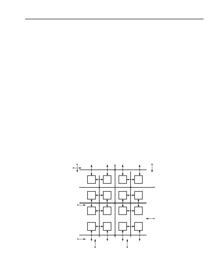
Figure 32 is a high-level diagram of the Series 3 system
clock spine network with sample xL line
connections for a 4 x 4 array of PLCs.
The clock spine structure previously described pro-
vides for complete distribution of a clock from any I/O
pin to the entire PLC array by means of a single clock
spine and long lines (xL). This distribution system also
provides a means to have many different clocks routed
to many different and dispersed locations in the PLC
array. Each spine can carry a different clock signal, so
for the OR3T55 (which has an 18 x 18 array of PLCs,
implying nine clock spines per side), 36 input clock sig-
nals can be supported using the system clock network.
Fast Clock
Fast clocks are high-speed, low-skew clock spines that
originate from the CLKCNTRL special function blocks
(described later). There are four fast clock spines—one
originating on the middle of each edge of the array. The
spines run in the interquad region of the PLC array
from their source side of the device to the last row or
column on the opposite side of the device. The fast
clocks connect to two long lines, xL[8] and xL[9], that
run orthogonal to the spine direction in each PLC.
These long lines can then be connected to the PFU
clock input in the same manner as the general system
clocks, and, like the system clock connections, xL lines
are only needed in every other row (column) to distrib-
ute a clock to every PFU. The limited number of long-
line connections and the low skew of the CLKCNTRL
source combine to make the fast clocks a very robust,
low-skew clock source.
5-5801(F).a
Figure 32.
ORCA Series 3 System Clock Distribution Overview
(xL)
HORIZONTAL
(xL)
UNUSED
(xL)
UNUSED
SCLK SPINE
(xL)
UNUSED
SCLK SPINE
VERTICAL
SCLK SPINE
UNUSED
SCLK SPINE
UNUSED
SCLK SPINE
UNUSED
SCLK SPINE
UNUSED
SCLK SPINE
UNUSED
SCLK SPINE
Select
devices
have
been
discontinued.
See
Ordering
Information
section
for
product
status.
相關(guān)PDF資料 |
PDF描述 |
|---|---|
| OR3T807PS240-DB | FPGA, 484 CLBS, 116000 GATES, PQFP240 |
| OR3T55-4BA256I | FPGA, 324 CLBS, 40000 GATES, 80 MHz, PBGA256 |
| OR3T55-4BA256 | FPGA, 324 CLBS, 40000 GATES, 80 MHz, PBGA256 |
| OR3T55-4BA352I | FPGA, 324 CLBS, 40000 GATES, 80 MHz, PBGA352 |
| OR3T55-4BA352 | FPGA, 324 CLBS, 40000 GATES, 80 MHz, PBGA352 |
相關(guān)代理商/技術(shù)參數(shù) |
參數(shù)描述 |
|---|---|
| OR3T80-6PS240I | 制造商:AGERE 制造商全稱:AGERE 功能描述:3C and 3T Field-Programmable Gate Arrays |
| OR3T806PS240I-DB | 功能描述:FPGA - 現(xiàn)場可編程門陣列 3872 LUT 342 I/O RoHS:否 制造商:Altera Corporation 系列:Cyclone V E 柵極數(shù)量: 邏輯塊數(shù)量:943 內(nèi)嵌式塊RAM - EBR:1956 kbit 輸入/輸出端數(shù)量:128 最大工作頻率:800 MHz 工作電源電壓:1.1 V 最大工作溫度:+ 70 C 安裝風(fēng)格:SMD/SMT 封裝 / 箱體:FBGA-256 |
| OR3T806S208-DB | 功能描述:FPGA - 現(xiàn)場可編程門陣列 Use LatticeEC RoHS:否 制造商:Altera Corporation 系列:Cyclone V E 柵極數(shù)量: 邏輯塊數(shù)量:943 內(nèi)嵌式塊RAM - EBR:1956 kbit 輸入/輸出端數(shù)量:128 最大工作頻率:800 MHz 工作電源電壓:1.1 V 最大工作溫度:+ 70 C 安裝風(fēng)格:SMD/SMT 封裝 / 箱體:FBGA-256 |
| OR3T806S208I-DB | 功能描述:FPGA - 現(xiàn)場可編程門陣列 Use LatticeEC RoHS:否 制造商:Altera Corporation 系列:Cyclone V E 柵極數(shù)量: 邏輯塊數(shù)量:943 內(nèi)嵌式塊RAM - EBR:1956 kbit 輸入/輸出端數(shù)量:128 最大工作頻率:800 MHz 工作電源電壓:1.1 V 最大工作溫度:+ 70 C 安裝風(fēng)格:SMD/SMT 封裝 / 箱體:FBGA-256 |
| OR3T80-7BA352 | 制造商:Lattice Semiconductor Corporation 功能描述:Field-Programmable Gate Array, 484 Cell, 352 Pin, Plastic, BGA |
發(fā)布緊急采購,3分鐘左右您將得到回復(fù)。