- 您現(xiàn)在的位置:買賣IC網(wǎng) > PDF目錄299575 > OR3C804BA352-DB (LATTICE SEMICONDUCTOR CORP) FPGA, 484 CLBS, 116000 GATES, PBGA352 PDF資料下載
參數(shù)資料
| 型號(hào): | OR3C804BA352-DB |
| 廠商: | LATTICE SEMICONDUCTOR CORP |
| 元件分類: | FPGA |
| 英文描述: | FPGA, 484 CLBS, 116000 GATES, PBGA352 |
| 封裝: | PLASTIC, BGA-352 |
| 文件頁(yè)數(shù): | 54/203頁(yè) |
| 文件大小: | 1368K |
| 代理商: | OR3C804BA352-DB |
第1頁(yè)第2頁(yè)第3頁(yè)第4頁(yè)第5頁(yè)第6頁(yè)第7頁(yè)第8頁(yè)第9頁(yè)第10頁(yè)第11頁(yè)第12頁(yè)第13頁(yè)第14頁(yè)第15頁(yè)第16頁(yè)第17頁(yè)第18頁(yè)第19頁(yè)第20頁(yè)第21頁(yè)第22頁(yè)第23頁(yè)第24頁(yè)第25頁(yè)第26頁(yè)第27頁(yè)第28頁(yè)第29頁(yè)第30頁(yè)第31頁(yè)第32頁(yè)第33頁(yè)第34頁(yè)第35頁(yè)第36頁(yè)第37頁(yè)第38頁(yè)第39頁(yè)第40頁(yè)第41頁(yè)第42頁(yè)第43頁(yè)第44頁(yè)第45頁(yè)第46頁(yè)第47頁(yè)第48頁(yè)第49頁(yè)第50頁(yè)第51頁(yè)第52頁(yè)第53頁(yè)當(dāng)前第54頁(yè)第55頁(yè)第56頁(yè)第57頁(yè)第58頁(yè)第59頁(yè)第60頁(yè)第61頁(yè)第62頁(yè)第63頁(yè)第64頁(yè)第65頁(yè)第66頁(yè)第67頁(yè)第68頁(yè)第69頁(yè)第70頁(yè)第71頁(yè)第72頁(yè)第73頁(yè)第74頁(yè)第75頁(yè)第76頁(yè)第77頁(yè)第78頁(yè)第79頁(yè)第80頁(yè)第81頁(yè)第82頁(yè)第83頁(yè)第84頁(yè)第85頁(yè)第86頁(yè)第87頁(yè)第88頁(yè)第89頁(yè)第90頁(yè)第91頁(yè)第92頁(yè)第93頁(yè)第94頁(yè)第95頁(yè)第96頁(yè)第97頁(yè)第98頁(yè)第99頁(yè)第100頁(yè)第101頁(yè)第102頁(yè)第103頁(yè)第104頁(yè)第105頁(yè)第106頁(yè)第107頁(yè)第108頁(yè)第109頁(yè)第110頁(yè)第111頁(yè)第112頁(yè)第113頁(yè)第114頁(yè)第115頁(yè)第116頁(yè)第117頁(yè)第118頁(yè)第119頁(yè)第120頁(yè)第121頁(yè)第122頁(yè)第123頁(yè)第124頁(yè)第125頁(yè)第126頁(yè)第127頁(yè)第128頁(yè)第129頁(yè)第130頁(yè)第131頁(yè)第132頁(yè)第133頁(yè)第134頁(yè)第135頁(yè)第136頁(yè)第137頁(yè)第138頁(yè)第139頁(yè)第140頁(yè)第141頁(yè)第142頁(yè)第143頁(yè)第144頁(yè)第145頁(yè)第146頁(yè)第147頁(yè)第148頁(yè)第149頁(yè)第150頁(yè)第151頁(yè)第152頁(yè)第153頁(yè)第154頁(yè)第155頁(yè)第156頁(yè)第157頁(yè)第158頁(yè)第159頁(yè)第160頁(yè)第161頁(yè)第162頁(yè)第163頁(yè)第164頁(yè)第165頁(yè)第166頁(yè)第167頁(yè)第168頁(yè)第169頁(yè)第170頁(yè)第171頁(yè)第172頁(yè)第173頁(yè)第174頁(yè)第175頁(yè)第176頁(yè)第177頁(yè)第178頁(yè)第179頁(yè)第180頁(yè)第181頁(yè)第182頁(yè)第183頁(yè)第184頁(yè)第185頁(yè)第186頁(yè)第187頁(yè)第188頁(yè)第189頁(yè)第190頁(yè)第191頁(yè)第192頁(yè)第193頁(yè)第194頁(yè)第195頁(yè)第196頁(yè)第197頁(yè)第198頁(yè)第199頁(yè)第200頁(yè)第201頁(yè)第202頁(yè)第203頁(yè)
Lattice Semiconductor
147
Data Sheet
November 2006
ORCA Series 3C and 3T FPGAs
Pin Information
Pin Descriptions
This section describes the pins found on the Series 3 FPGAs. Any pin not described in this table is a user-program-
mable I/O. During conguration, the user-programmable I/Os are 3-stated with an internal pull-up resistor enabled.
If any pin is not used (or not bonded to a package pin), it is also 3-stated with an internal pull-up resistor enabled
after conguration.
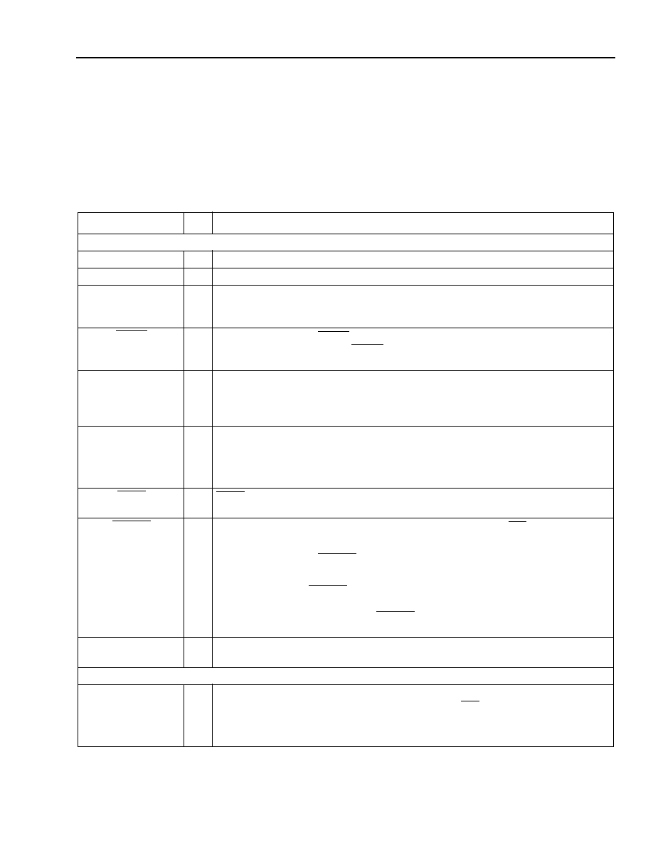
Table 67. Pin Descriptions
Symbol
I/O
Description
Dedicated Pins
VDD
—
Positive power supply.
GND
—
Ground supply.
VDD5
—
5 V tolerant select. VDD5 pin locations are shown for package compatibility with
OR2TxxA devices. Connections to 5 V power sources are not used for 5 V tolerant
I/Os in the OR3Txxx devices.
RESET
I
During conguration, RESET forces the restart of conguration and a pull-up is
enabled. After conguration, RESET can be used as a general FPGA input or as a
direct input, which causes all PLC latches/FFs to be asynchronously set/reset.
CCLK
I
In the master and asynchronous peripheral modes, CCLK is an output which
strobes conguration data in. In the slave or synchronous peripheral mode, CCLK
is input synchronous with the data on DIN or D[7:0]. In microprocessor mode, CCLK
is used internally and output for daisy-chain operation.
DONE
I
O
As an input, a low level on DONE delays FPGA start-up after conguration (see
Note).
As an active-high, open-drain output, a high level on this signal indicates that cong-
uration is complete. DONE has an optional pull-up resistor.
PRGM
I
PRGM
is an active-low input that forces the restart of conguration and resets the
boundary-scan circuitry. This pin always has an active pull-up.
RD_CFG
I
This pin must be held high during device initialization until the INIT pin goes high.
This pin always has an active pull-up.
During conguration, RD_CFG is an active-low input that activates the TS_ALL func-
tion and 3-states all of the I/O.
After conguration, RD_CFG can be selected (via a bit stream option) to activate the
TS_ALL function as described above, or, if readback is enabled via a bit stream
option, a high-to-low transition on RD_CFG will initiate readback of the conguration
data, including PFU output states, starting with frame address 0.
RD_DATA/TDO
O
RD_DATA/TDO is a dual-function pin. If used for readback, RD_DATA provides con-
guration data out. If used in boundary scan, TDO is test data out.
Special-Purpose Pins
M0, M1, M2
I
I/O
During powerup and initialization, M0—M2 are used to select the conguration
uration modes. During conguration, a pull-up is enabled.
After conguration, these pins are user-programmable I/O (see Note).
Note: The FPGA States of Operation section contains more information on how to control these signals during start-up. The timing of DONE
release is controlled by one set of bit stream options, and the timing of the simultaneous release of all other conguration pins (and the
activation of all user I/Os) is controlled by a second set of options.
Select
devices
have
been
discontinued.
See
Ordering
Information
section
for
product
status.
相關(guān)PDF資料 |
PDF描述 |
|---|---|
| OR3C804PS208-DB | FPGA, 484 CLBS, 116000 GATES, PQFP208 |
| OR3T1256PS208I-DB | FPGA, 784 CLBS, 186000 GATES, PQFP208 |
| OR3T1256PS240-DB | FPGA, 784 CLBS, 186000 GATES, PQFP240 |
| OR3T1256PS240I-DB | FPGA, 784 CLBS, 186000 GATES, PQFP240 |
| OR3T1257PS208-DB | FPGA, 784 CLBS, 186000 GATES, PQFP208 |
相關(guān)代理商/技術(shù)參數(shù) |
參數(shù)描述 |
|---|---|
| OR3C80-4BA352I | 制造商:AGERE 制造商全稱:AGERE 功能描述:3C and 3T Field-Programmable Gate Arrays |
| OR3C804BA352I-DB | 功能描述:FPGA - 現(xiàn)場(chǎng)可編程門陣列 3872 LUT 356 I/O RoHS:否 制造商:Altera Corporation 系列:Cyclone V E 柵極數(shù)量: 邏輯塊數(shù)量:943 內(nèi)嵌式塊RAM - EBR:1956 kbit 輸入/輸出端數(shù)量:128 最大工作頻率:800 MHz 工作電源電壓:1.1 V 最大工作溫度:+ 70 C 安裝風(fēng)格:SMD/SMT 封裝 / 箱體:FBGA-256 |
| OR3C80-4BC432 | 制造商:AGERE 制造商全稱:AGERE 功能描述:3C and 3T Field-Programmable Gate Arrays |
| OR3C80-4BC432I | 制造商:AGERE 制造商全稱:AGERE 功能描述:3C and 3T Field-Programmable Gate Arrays |
| OR3C80-4BC600I | 制造商:未知廠家 制造商全稱:未知廠家 功能描述:Field Programmable Gate Array (FPGA) |
發(fā)布緊急采購(gòu),3分鐘左右您將得到回復(fù)。