- 您現(xiàn)在的位置:買賣IC網(wǎng) > PDF目錄359236 > MTD20N03HDL (MOTOROLA INC) TMOS POWER FET LOGIC LEVEL 20 AMPERES 30 VOLTS RDS(on) = 0.035 OHM PDF資料下載
參數(shù)資料
| 型號(hào): | MTD20N03HDL |
| 廠商: | MOTOROLA INC |
| 元件分類: | JFETs |
| 英文描述: | TMOS POWER FET LOGIC LEVEL 20 AMPERES 30 VOLTS RDS(on) = 0.035 OHM |
| 中文描述: | 20 A, 30 V, 0.04 ohm, N-CHANNEL, Si, POWER, MOSFET |
| 封裝: | DPAK-3 |
| 文件頁數(shù): | 22/38頁 |
| 文件大小: | 739K |
| 代理商: | MTD20N03HDL |
第1頁第2頁第3頁第4頁第5頁第6頁第7頁第8頁第9頁第10頁第11頁第12頁第13頁第14頁第15頁第16頁第17頁第18頁第19頁第20頁第21頁當(dāng)前第22頁第23頁第24頁第25頁第26頁第27頁第28頁第29頁第30頁第31頁第32頁第33頁第34頁第35頁第36頁第37頁第38頁
Analog Integrated Circuit Device Data
Freescale Semiconductor
22
34701
FUNCTIONAL DESCRIPTION
FUNCTIONAL DEVICE OPERATION
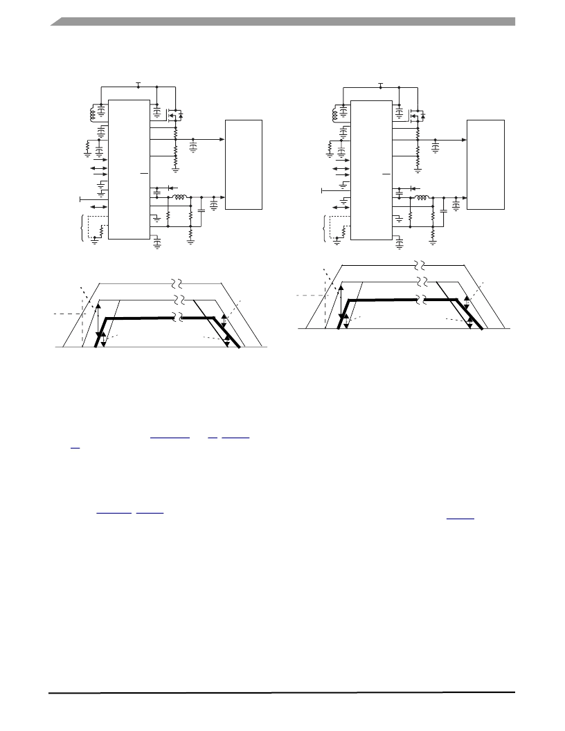
Figure 18. Standard Power Up/Down Sequence
in +5.0 V Supply System
STANDARD POWER SEQUENCING
When the power supply IC operates in the Standard Power
Sequencing mode, the switcher output provides the core
voltage for the microprocessor. This situation and operating
conditions are illustrated in
Figures 17
and
18
.
Table 5
,
page
16
, shows the Power Sequencing mode selection.
INVERTED POWER SEQUENCING
When the power supply IC is operating in the Inverted
Power Sequencing mode, the linear regulator (LDO) output
provides the core voltage for the microprocessor, as
illustrated in
Figure 19
.
Table 5
shows the Power
Sequencing mode selection.
Figure 19. Inverted Power Up/Down Sequence in +5.0 V
Supply System
ASSUMED REQUIREMENTS
1. I/O supply voltage not to exceed core voltage by more
than 2.0 V.
2. Core supply voltage not to exceed I/O voltage by more
than 0.4 V.
Methods of Control
The 34701 has several methods of monitoring and
controlling the regulator output voltages, as described in the
paragraphs below. Power sequencing control is also
achieved through the intrinsic operation of the regulators.
The EN1 and EN2 terminals can be used to select the proper
power sequencing mode required by the powered system or
to disable the power sequencing (refer to
Table 5
).
Intrinsic Operation
For both the LDO and switcher, whenever the output
voltage is below the regulation point, the LDO external Pass
MOSFET is on, or the Buck High-Side MOSFET is on at a
duty cycle controlled by the switcher. Because these devices
are MOSFETs, current can flow in either direction, balancing
the voltages via the common supply terminal. The ability to
maintain the MOSFETs on is dependent on the available gate
voltage, and thus the size of the boost regulator storage
capacitor.
V = 2.1 V
Max. Lead
V = 0.4 V
Max. Lag
V = 0.4 V
Max. Lag
1.8V Start-Up
3.3 V I/O Voltage (VLDO)
1.5 V Core Voltage
(VOUT)
5.0 V Input Supply
V = 2.1 V
Max. Lead
RT
VBD
VBST
VDDH (I/Os)
VDDL (Core)
MCU
34701
5.0 V Input
VIN2
CLKSEL
FREQ
GND
SDA
SCL
ADDR
VIN1
LDRV
CS
LDO
LFB
RST
SW
PGND
INV
BOOT
VOUT
CLKSYN
Optional
EN1
EN2
VBST
VDDI
3.3 V
1.5 V
5.0 V
V = 2.1 V
Max. Lead
V = 0.4 V
Max. Lag
V = 0.4 V
Max. Lag
1.8V Start-Up
3.3 V I/O Voltage (VOUT)
1.5 V Core Voltage(VLDO)
5.0 V Input Supply
V = 2.1 V
Max. Lead
RT
VBD
VBST
VDDH (I/Os)
VDDL (Core)
MCU
34701
5.0 V Input
VIN2
CLKSEL
FREQ
GND
SDA
SCL
ADDR
VIN1
LDRV
CS
LDO
LFB
RST
SW
PGND
INV
BOOT
VOUT
CLKSYN
Optional
EN1
EN2
VBST
VDDI
3.3 V
1.5 V
5.0 V
相關(guān)PDF資料 |
PDF描述 |
|---|---|
| MTD20N03HL | HDTMOS E-FET High Density Power FET DPAK for Surface Mount |
| MTH-50 | Two-Way Power Dividers 1 - 100 MHz and 40 - 400 MHz |
| MTH-50PIN | Two-Way Power Dividers 1 - 100 MHz and 40 - 400 MHz |
| MTP3N60 | N - CHANNEL ENHANCEMENT MODE POWER MOS TRANSISTOR |
| MTVX2602 | Managed 24 Port 10/100 Mbps Ethernet Switch |
相關(guān)代理商/技術(shù)參數(shù) |
參數(shù)描述 |
|---|---|
| MTD20N03HDLT4 | 制造商:ON Semiconductor 功能描述:Trans MOSFET N-CH 30V 20A 3-Pin(2+Tab) DPAK T/R |
| MTD20N03HL | 制造商:Motorola Inc 功能描述:20N03HL |
| MTD20N06 | 制造商:MOTOROLA 制造商全稱:Motorola, Inc 功能描述:TMOS POWER FET 20 AMPERES 60 VOLTS RDS(on) = 0.080 OHM |
| MTD20N06HD | 制造商:ON Semiconductor 功能描述:Trans MOSFET N-CH 60V 20A 3-Pin(2+Tab) DPAK Rail 制造商:ON Semiconductor 功能描述:MOSFET N D-PAK |
| MTD20N06HD-1 | 制造商:ONSEMI 制造商全稱:ON Semiconductor 功能描述:Power MOSFET 20 Amps, 60 Volts N−Channel DPAK |
發(fā)布緊急采購,3分鐘左右您將得到回復(fù)。