- 您現(xiàn)在的位置:買賣IC網(wǎng) > PDF目錄384755 > MT48LC2M32B2 (Micron Technology, Inc.) SYNCHRONOUS DRAM PDF資料下載
參數(shù)資料
| 型號(hào): | MT48LC2M32B2 |
| 廠商: | Micron Technology, Inc. |
| 英文描述: | SYNCHRONOUS DRAM |
| 中文描述: | 同步DRAM |
| 文件頁數(shù): | 13/53頁 |
| 文件大?。?/td> | 1818K |
| 代理商: | MT48LC2M32B2 |
第1頁第2頁第3頁第4頁第5頁第6頁第7頁第8頁第9頁第10頁第11頁第12頁當(dāng)前第13頁第14頁第15頁第16頁第17頁第18頁第19頁第20頁第21頁第22頁第23頁第24頁第25頁第26頁第27頁第28頁第29頁第30頁第31頁第32頁第33頁第34頁第35頁第36頁第37頁第38頁第39頁第40頁第41頁第42頁第43頁第44頁第45頁第46頁第47頁第48頁第49頁第50頁第51頁第52頁第53頁
13
64Mb: x32 SDRAM
64MSDRAMx32_5.p65 – Rev. B; Pub. 6/02
Micron Technology, Inc., reserves the right to change products or specifications without notice.
2002, Micron Technology, Inc.
64Mb: x32
SDRAM
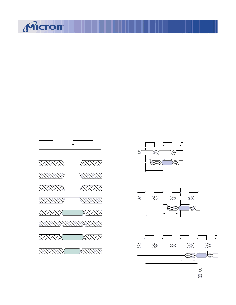
Upon completion of a burst, assuming no other com-
mands have been initiated, the DQs will go High-Z. A
full-page burst will continue until terminated. (At the
end of the page, it will wrap to column 0 and continue.)
Data from any READ burst may be truncated with a
subsequent READ command, and data from a fixed-
length READ burst may be immediately followed by
data from a READ command. In either case, a continu-
ous flow of data can be maintained. The first data ele-
ment from the new burst follows either the last ele-
ment of a completed burst or the last desired data ele-
ment of a longer burst that is being truncated. The new
READ command should be issued
x
cycles before the
clock edge at which the last desired data element is
valid, where
x
equals the CAS latency minus one. This
is shown in Figure 7 for CAS latencies of one, two and
READs
READ bursts are initiated with a READ command,
as shown in Figure 5.
The starting column and bank addresses are pro-
vided with the READ command, and auto precharge is
either enabled or disabled for that burst access. If auto
precharge is enabled, the row being accessed is
precharged at the completion of the burst. For the ge-
neric READ commands used in the following illustra-
tions, auto precharge is disabled.
During READ bursts, the valid data-out element
from the starting column address will be available fol-
lowing the CAS latency after the READ command. Each
subsequent data-out element will be valid by the next
positive clock edge. Figure 6 shows general timing for
each possible CAS latency setting.
Figure 5
READ Command
Figure 6
CAS Latency
CLK
DQ
T2
T1
T3
T0
CAS Latency = 3
LZ
D
OUT
tOH
t
COMMAND
NOP
READ
tAC
NOP
T4
NOP
DON’T CARE
UNDEFINED
CLK
DQ
T2
T1
T0
CAS Latency = 1
LZ
D
OUT
tOH
t
COMMAND
NOP
READ
tAC
CLK
DQ
T2
T1
T3
T0
CAS Latency = 2
LZ
D
OUT
tOH
t
COMMAND
NOP
READ
tAC
NOP
CS#
WE#
CAS#
RAS#
CKE
CLK
COLUMN
ADDRESS
A0–A7
A10
BA0, 1
HIGH
ENABLE AUTO PRECHARGE
DISABLE AUTO PRECHARGE
BANK
ADDRESS
A8, A9
相關(guān)PDF資料 |
PDF描述 |
|---|---|
| MT48LC32M8A2 | SYNCHRONOUS DRAM |
| MT48LC16M16A2 | SYNCHRONOUS DRAM |
| MT48LC64M4A2 | SYNCHRONOUS DRAM |
| MT48LC4M32B2 | SYNCHRONOUS DRAM |
| MT48LC4M32LFFC | SYNCHRONOUS DRAM |
相關(guān)代理商/技術(shù)參數(shù) |
參數(shù)描述 |
|---|---|
| MT48LC2M32B2-6G | 制造商:Micron Technology Inc 功能描述: |
發(fā)布緊急采購,3分鐘左右您將得到回復(fù)。