- 您現(xiàn)在的位置:買(mǎi)賣(mài)IC網(wǎng) > PDF目錄383632 > mPD705101 (NEC Corp.) V831TM 32-BIT MICROPROCESSOR PDF資料下載
參數(shù)資料
| 型號(hào): | mPD705101 |
| 廠商: | NEC Corp. |
| 英文描述: | V831TM 32-BIT MICROPROCESSOR |
| 中文描述: | V831TM 32位微處理器 |
| 文件頁(yè)數(shù): | 43/72頁(yè) |
| 文件大小: | 302K |
| 代理商: | MPD705101 |
第1頁(yè)第2頁(yè)第3頁(yè)第4頁(yè)第5頁(yè)第6頁(yè)第7頁(yè)第8頁(yè)第9頁(yè)第10頁(yè)第11頁(yè)第12頁(yè)第13頁(yè)第14頁(yè)第15頁(yè)第16頁(yè)第17頁(yè)第18頁(yè)第19頁(yè)第20頁(yè)第21頁(yè)第22頁(yè)第23頁(yè)第24頁(yè)第25頁(yè)第26頁(yè)第27頁(yè)第28頁(yè)第29頁(yè)第30頁(yè)第31頁(yè)第32頁(yè)第33頁(yè)第34頁(yè)第35頁(yè)第36頁(yè)第37頁(yè)第38頁(yè)第39頁(yè)第40頁(yè)第41頁(yè)第42頁(yè)當(dāng)前第43頁(yè)第44頁(yè)第45頁(yè)第46頁(yè)第47頁(yè)第48頁(yè)第49頁(yè)第50頁(yè)第51頁(yè)第52頁(yè)第53頁(yè)第54頁(yè)第55頁(yè)第56頁(yè)第57頁(yè)第58頁(yè)第59頁(yè)第60頁(yè)第61頁(yè)第62頁(yè)第63頁(yè)第64頁(yè)第65頁(yè)第66頁(yè)第67頁(yè)第68頁(yè)第69頁(yè)第70頁(yè)第71頁(yè)第72頁(yè)
μ
PD705101
43
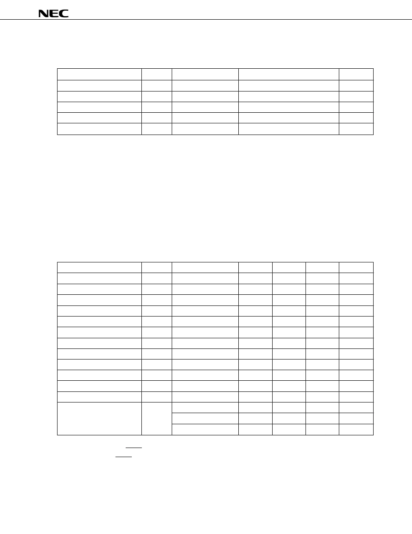
16. ELECTRICAL SPECIFICATIONS
ABSOLUTE MAXIMUM RATINGS (T
A
= 25C)
Parameter
Symbol
Conditions
Rating
Unit
Power supply voltage
V
DD
–0.5 to +4.5
V
Input voltage
V
I
–0.5 to V
DD
+ 0.3
V
Clock input voltage
V
K
–0.5 to V
DD
+ 0.3
V
Operating ambient temperature
V
A
–40 to +85
C
Storage temperature
T
stg
–65 to +150
C
Cautions 1. Do not connect an output (or input/output) pin of an IC device directly to any other output (or
input/output) pin of the same device. Do not connect the V
DD
or V
CC
pin of an IC device directly
to its GND pin or a ground. Note, however, that these restrictions do not apply to the high-
impedance pins of an external circuit, whose timing has been specifically designed to avoid
output collision.
2. Absolute maximum ratings are rated values, beyond which physical damage may be caused
to the product; if the rated value of any of the parameters in the above table is exceeded even
momentarily, the quality of the product may deteriorate. Always use the product within its rated
values, therefore. For IC products, normal operation and quality are guaranteed only when
the ratings and conditions described under the DC and AC characteristics are satisfied.
DC CHARACTERISTICS (T
A
= –40 to +85C, V
DD
= 3.0 to 3.6 V)
Parameter
Symbol
Conditions
MIN.
TYP.
MAX.
Unit
Low-level clock input voltage
V
KL
Note 1
–0.5
+0.2 V
DD
V
High-level clock input voltage
V
KH
Note 1
0.8 V
DD
V
DD
+ 0.3
V
Low-level input voltage
V
IL
–0.5
+0.6
V
High-level input voltage
V
IH
2.0
V
DD
+ 0.3
V
Low-level shmitt input voltage
V
SL
Note 2
–0.5
+0.2 V
DD
V
High-level shmitt input voltage
V
SH
Note 2
0.8 V
DD
V
DD
+ 0.3
V
Low-level output voltage
V
OL
I
OL
= 3.2 mA
0.4
V
High-level output voltage
V
OH
I
OH
= –400
μ
A
0.85 V
DD
V
Low-level input leakage current
I
LIL
V
I
= 0 V
–10
μ
A
High-level input leakage current
I
LIH
V
IN
= V
DD
10
μ
A
Low-level output leakage current
I
LOL
V
O
= 0 V
–10
μ
A
High-level output leakage current
I
LOH
V
O
= V
DD
10
μ
A
Supply current
Note 3
I
DD
When operating
167
230
mA
At HALT mode
45
60
mA
At STOP mode
Note 4
36
180
μ
A
Notes 1.
X2 pin and SCLK pin at external clock input
2.
PORT0/SCLK, PORT2/SI, RXD
3.
Supply current at f = 33 MHz, when output pins are open.
4.
External clock mode when clock input is stopped.
相關(guān)PDF資料 |
PDF描述 |
|---|---|
| mPD705101GM-100-8ED | V831TM 32-BIT MICROPROCESSOR |
| mPD784037 | 16/8-BIT SINGLE-CHIP MICROCONTROLLER |
| mPD784031 | 16/8-BIT SINGLE-CHIP MICROCONTROLLER |
| mPD784035 | 16/8-BIT SINGLE-CHIP MICROCONTROLLER |
| mPD784036 | 16/8-BIT SINGLE-CHIP MICROCONTROLLER |
相關(guān)代理商/技術(shù)參數(shù) |
參數(shù)描述 |
|---|---|
| MPD705101GM-100-8ED | 制造商:NEC 制造商全稱:NEC 功能描述:V831TM 32-BIT MICROPROCESSOR |
| MP-D70P-100/240V | 制造商:Panasonic Electric Works 功能描述: |
| MPD784031 | 制造商:NEC 制造商全稱:NEC 功能描述:16/8-BIT SINGLE-CHIP MICROCONTROLLER |
| MPD784035 | 制造商:NEC 制造商全稱:NEC 功能描述:16/8-BIT SINGLE-CHIP MICROCONTROLLER |
| MPD784036 | 制造商:NEC 制造商全稱:NEC 功能描述:16/8-BIT SINGLE-CHIP MICROCONTROLLER |
發(fā)布緊急采購(gòu),3分鐘左右您將得到回復(fù)。