- 您現(xiàn)在的位置:買賣IC網(wǎng) > PDF目錄382338 > MMBT589LT1 (ON SEMICONDUCTOR) High Current Surface Mount PNP Silicon Switching Transistor PDF資料下載
參數(shù)資料
| 型號: | MMBT589LT1 |
| 廠商: | ON SEMICONDUCTOR |
| 元件分類: | 小信號晶體管 |
| 英文描述: | High Current Surface Mount PNP Silicon Switching Transistor |
| 中文描述: | 1000 mA, 30 V, PNP, Si, SMALL SIGNAL TRANSISTOR, TO-236AB |
| 封裝: | CASE 318-08, TO-236, 3 PIN |
| 文件頁數(shù): | 5/8頁 |
| 文件大小: | 66K |
| 代理商: | MMBT589LT1 |
MMBT589LT1
http://onsemi.com
5
The values for the equation are found in the maximum
ratings table on the data sheet. Substituting these values
into the equation for an ambient temperature TA of 25
°
C,
one can calculate the power dissipation of the device which
in this case is 225 milliwatts.
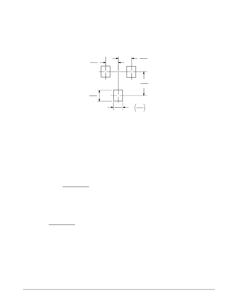
INFORMATION FOR USING THE SOT–23 SURFACE MOUNT PACKAGE
MINIMUM RECOMMENDED FOOTPRINT FOR SURFACE MOUNTED APPLICATIONS
Surface mount board layout is a critical portion of the
total design. The footprint for the semiconductor packages
must be the correct size to insure proper solder connection
interface between the board and the package. With the
correct pad geometry, the packages will self align when
subjected to a solder reflow process.
SOT–23
mm
inches
0.037
0.95
0.037
0.95
0.079
2.0
0.035
0.9
0.031
0.8
SOT–23 POWER DISSIPATION
PD =
TJ(max) – TA
R
θ
JA
PD =
150
°
C – 25
°
C
556
°
C/W
= 225 milliwatts
The power dissipation of the SOT–23 is a function of the
pad size. This can vary from the minimum pad size for
soldering to a pad size given for maximum power dissipa-
tion. Power dissipation for a surface mount device is deter-
mined by TJ(max), the maximum rated junction temperature
of the die, R
θ
JA, the thermal resistance from the device
junction to ambient, and the operating temperature, TA.
Using the values provided on the data sheet for the SOT–23
package, PD can be calculated as follows:
The 556
°
C/W for the SOT–23 package assumes the use
of the recommended footprint on a glass epoxy printed
circuit board to achieve a power dissipation of 225 milli-
watts. There are other alternatives to achieving higher
power dissipation from the SOT–23 package. Another
alternative would be to use a ceramic substrate or an
aluminum core board such as Thermal Clad
. Using a
board material such as Thermal Clad, an aluminum core
board, the power dissipation can be doubled using the same
footprint.
SOLDERING PRECAUTIONS
The melting temperature of solder is higher than the
rated temperature of the device. When the entire device is
heated to a high temperature, failure to complete soldering
within a short time could result in device failure. There-
fore, the following items should always be observed in
order to minimize the thermal stress to which the devices
are subjected.
Always preheat the device.
The delta temperature between the preheat and
soldering should be 100
°
C or less.*
When preheating and soldering, the temperature of the
leads and the case must not exceed the maximum
temperature ratings as shown on the data sheet. When
using infrared heating with the reflow soldering
method, the difference shall be a maximum of 10
°
C.
The soldering temperature and time shall not exceed
260
°
C for more than 10 seconds.
When shifting from preheating to soldering, the
maximum temperature gradient shall be 5
°
C or less.
After soldering has been completed, the device should
be allowed to cool naturally for at least three minutes.
Gradual cooling should be used as the use of forced
cooling will increase the temperature gradient and
result in latent failure due to mechanical stress.
Mechanical stress or shock should not be applied
during cooling.
* Soldering a device without preheating can cause exces-
sive thermal shock and stress which can result in damage
to the device.
相關(guān)PDF資料 |
PDF描述 |
|---|---|
| MMBTA28-7 | MicroPower Single-Supply Operational Amplifier MicroAmplifier(TM) Series 14-TSSOP |
| MMBTA28 | MicroPower Single-Supply Operational Amplifier MicroAmplifier(TM) Series 14-TSSOP |
| MMBTH10-4LT1 | VHF/UHF Transistor (NPN Silicon) |
| MMBTH10L | VHF/UHF Transistor |
| MMBTH10LT1 | VHF/UHF Transistor |
相關(guān)代理商/技術(shù)參數(shù) |
參數(shù)描述 |
|---|---|
| MMBT589LT1G | 功能描述:兩極晶體管 - BJT 2A 30V Switching PNP RoHS:否 制造商:STMicroelectronics 配置: 晶體管極性:PNP 集電極—基極電壓 VCBO: 集電極—發(fā)射極最大電壓 VCEO:- 40 V 發(fā)射極 - 基極電壓 VEBO:- 6 V 集電極—射極飽和電壓: 最大直流電集電極電流: 增益帶寬產(chǎn)品fT: 直流集電極/Base Gain hfe Min:100 A 最大工作溫度: 安裝風(fēng)格:SMD/SMT 封裝 / 箱體:PowerFLAT 2 x 2 |
| MMBT589LT3 | 功能描述:兩極晶體管 - BJT 2A 30V Switching PNP RoHS:否 制造商:STMicroelectronics 配置: 晶體管極性:PNP 集電極—基極電壓 VCBO: 集電極—發(fā)射極最大電壓 VCEO:- 40 V 發(fā)射極 - 基極電壓 VEBO:- 6 V 集電極—射極飽和電壓: 最大直流電集電極電流: 增益帶寬產(chǎn)品fT: 直流集電極/Base Gain hfe Min:100 A 最大工作溫度: 安裝風(fēng)格:SMD/SMT 封裝 / 箱體:PowerFLAT 2 x 2 |
| MMBT589LT3G | 功能描述:兩極晶體管 - BJT 2A 30V Switching PNP RoHS:否 制造商:STMicroelectronics 配置: 晶體管極性:PNP 集電極—基極電壓 VCBO: 集電極—發(fā)射極最大電壓 VCEO:- 40 V 發(fā)射極 - 基極電壓 VEBO:- 6 V 集電極—射極飽和電壓: 最大直流電集電極電流: 增益帶寬產(chǎn)品fT: 直流集電極/Base Gain hfe Min:100 A 最大工作溫度: 安裝風(fēng)格:SMD/SMT 封裝 / 箱體:PowerFLAT 2 x 2 |
| MMBT5962 | 功能描述:兩極晶體管 - BJT NPN Transistor General Purpose RoHS:否 制造商:STMicroelectronics 配置: 晶體管極性:PNP 集電極—基極電壓 VCBO: 集電極—發(fā)射極最大電壓 VCEO:- 40 V 發(fā)射極 - 基極電壓 VEBO:- 6 V 集電極—射極飽和電壓: 最大直流電集電極電流: 增益帶寬產(chǎn)品fT: 直流集電極/Base Gain hfe Min:100 A 最大工作溫度: 安裝風(fēng)格:SMD/SMT 封裝 / 箱體:PowerFLAT 2 x 2 |
| MMBT5962_Q | 功能描述:兩極晶體管 - BJT NPN Transistor General Purpose RoHS:否 制造商:STMicroelectronics 配置: 晶體管極性:PNP 集電極—基極電壓 VCBO: 集電極—發(fā)射極最大電壓 VCEO:- 40 V 發(fā)射極 - 基極電壓 VEBO:- 6 V 集電極—射極飽和電壓: 最大直流電集電極電流: 增益帶寬產(chǎn)品fT: 直流集電極/Base Gain hfe Min:100 A 最大工作溫度: 安裝風(fēng)格:SMD/SMT 封裝 / 箱體:PowerFLAT 2 x 2 |
發(fā)布緊急采購,3分鐘左右您將得到回復(fù)。