- 您現(xiàn)在的位置:買(mǎi)賣(mài)IC網(wǎng) > PDF目錄1949 > MC68LC060RC66 (Freescale Semiconductor)IC MPU 32BIT 66MHZ 206-PGA PDF資料下載
參數(shù)資料
| 型號(hào): | MC68LC060RC66 |
| 廠(chǎng)商: | Freescale Semiconductor |
| 文件頁(yè)數(shù): | 7/128頁(yè) |
| 文件大小: | 0K |
| 描述: | IC MPU 32BIT 66MHZ 206-PGA |
| 標(biāo)準(zhǔn)包裝: | 10 |
| 系列: | M680x0 |
| 處理器類(lèi)型: | M680x0 32-位 |
| 速度: | 66MHz |
| 電壓: | 3.3V |
| 安裝類(lèi)型: | 通孔 |
| 封裝/外殼: | 206-BEPGA |
| 供應(yīng)商設(shè)備封裝: | 206-PGA(47.25x47.25) |
| 包裝: | 托盤(pán) |
第1頁(yè)第2頁(yè)第3頁(yè)第4頁(yè)第5頁(yè)第6頁(yè)當(dāng)前第7頁(yè)第8頁(yè)第9頁(yè)第10頁(yè)第11頁(yè)第12頁(yè)第13頁(yè)第14頁(yè)第15頁(yè)第16頁(yè)第17頁(yè)第18頁(yè)第19頁(yè)第20頁(yè)第21頁(yè)第22頁(yè)第23頁(yè)第24頁(yè)第25頁(yè)第26頁(yè)第27頁(yè)第28頁(yè)第29頁(yè)第30頁(yè)第31頁(yè)第32頁(yè)第33頁(yè)第34頁(yè)第35頁(yè)第36頁(yè)第37頁(yè)第38頁(yè)第39頁(yè)第40頁(yè)第41頁(yè)第42頁(yè)第43頁(yè)第44頁(yè)第45頁(yè)第46頁(yè)第47頁(yè)第48頁(yè)第49頁(yè)第50頁(yè)第51頁(yè)第52頁(yè)第53頁(yè)第54頁(yè)第55頁(yè)第56頁(yè)第57頁(yè)第58頁(yè)第59頁(yè)第60頁(yè)第61頁(yè)第62頁(yè)第63頁(yè)第64頁(yè)第65頁(yè)第66頁(yè)第67頁(yè)第68頁(yè)第69頁(yè)第70頁(yè)第71頁(yè)第72頁(yè)第73頁(yè)第74頁(yè)第75頁(yè)第76頁(yè)第77頁(yè)第78頁(yè)第79頁(yè)第80頁(yè)第81頁(yè)第82頁(yè)第83頁(yè)第84頁(yè)第85頁(yè)第86頁(yè)第87頁(yè)第88頁(yè)第89頁(yè)第90頁(yè)第91頁(yè)第92頁(yè)第93頁(yè)第94頁(yè)第95頁(yè)第96頁(yè)第97頁(yè)第98頁(yè)第99頁(yè)第100頁(yè)第101頁(yè)第102頁(yè)第103頁(yè)第104頁(yè)第105頁(yè)第106頁(yè)第107頁(yè)第108頁(yè)第109頁(yè)第110頁(yè)第111頁(yè)第112頁(yè)第113頁(yè)第114頁(yè)第115頁(yè)第116頁(yè)第117頁(yè)第118頁(yè)第119頁(yè)第120頁(yè)第121頁(yè)第122頁(yè)第123頁(yè)第124頁(yè)第125頁(yè)第126頁(yè)第127頁(yè)第128頁(yè)
Caches
MOTOROLA
M68060 USER’S MANUAL
5-5
Operands of locked instructions (CAS and TAS) and operand references while the lock bit
in the bus control register is set which miss in the data cache do not allocate for reads or
writes regardless of the caching mode, and therefore will bypass the cache. Locked instruc-
tions that hit in the data cache invalidate a matching valid entry or will push and invalidate a
matching dirty entry. The locked operand access will then bypass the cache.
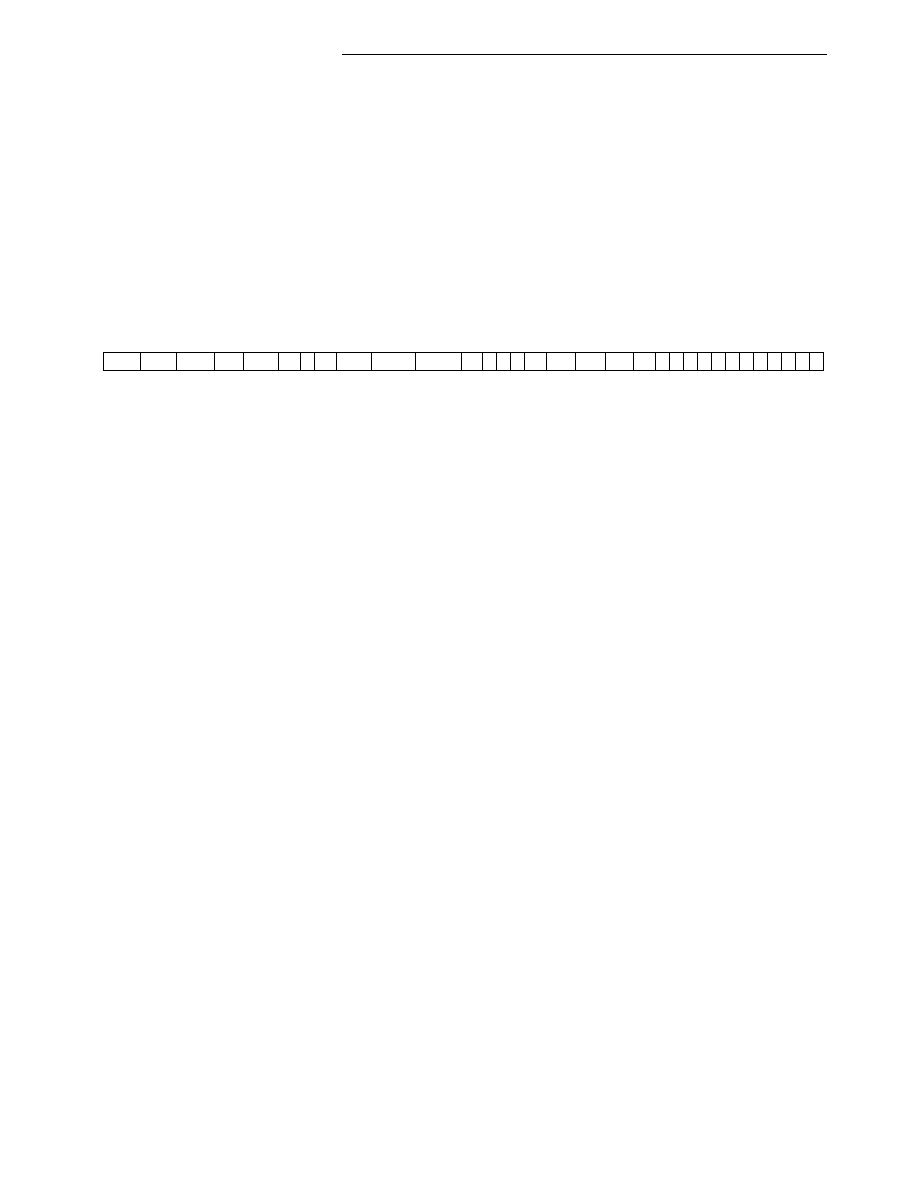
5.2 CACHE CONTROL REGISTER
The cache control register (CACR) is a 32-bit register which contains control information for
the instruction and data caches. A MOVEC sets all of the bits in the CACR. A hardware reset
clears the CACR, disabling both caches; however, reset does not affect the tags, state infor-
mation, and data within the caches. The CACR is illustrated in Figure 5-5.
EDC—Enable Data Cache
0 = Data cache is disabled.
1 = Data cache is enabled.
NAD—No Allocate Mode (Data Cache)
0 = Read and write misses will allocate in the data cache.
1 = Read and write misses will not allocate in the data cache.
ESB—Enable Store Buffer
0 = All writes to writethrough or cache-inhibited imprecise pages will bypass the store
buffer and generate bus cycles directly.
1 = The four entry first-in-first-out (FIFO) store buffer to the MC68060 is enabled. This
buffer is used to defer pending writes to writethrough or cache-inhibited imprecise
pages to maximize performance.
Locked write accesses and accesses to cache-inhibited precise pages always bypass the
store buffer.
DPI—Disable CPUSH Invalidation
0 = Each cache line is invalidated as it is pushed. Affects only the data cache.
1 = CPUSHed lines remain valid in the cache.
FOC—1/2 Cache Operation Mode Enable (Data Cache)
0 = The data cache operates in normal, full-cache mode.
1 = The data cache operates in 1/2-cache mode.
31
30
29
28
27
26
24
23
22
21
20
16
15
14
13
12
0
EDC
NAD
ESB
DPI
FOC
0
EBC
CABC
CUBC
0
0 0 0
0
EIC
NAI
FIC
0
000000000000
Figure 5-5. Cache Control Register
相關(guān)PDF資料 |
PDF描述 |
|---|---|
| MC68LC060ZU75 | IC MPU 32BIT 68K 75MHZ 304-TBGA |
| MC68M360ZQ25VLR2 | IC MPU QUICC 25MHZ 357-PBGA |
| MC68MH360CZQ25L | IC MPU QUICC 25MHZ 357-PBGA |
| MC68P11E1CFNE2R | IC MCU 8BIT 52-PLCC |
| MC68SEC000AA16R2 | IC MPU 32BIT 16 MHZ 64-QFP |
相關(guān)代理商/技術(shù)參數(shù) |
參數(shù)描述 |
|---|---|
| MC68LC060RC75 | 功能描述:微處理器 - MPU 32B W/ CACHE MMU RoHS:否 制造商:Atmel 處理器系列:SAMA5D31 核心:ARM Cortex A5 數(shù)據(jù)總線(xiàn)寬度:32 bit 最大時(shí)鐘頻率:536 MHz 程序存儲(chǔ)器大小:32 KB 數(shù)據(jù) RAM 大小:128 KB 接口類(lèi)型:CAN, Ethernet, LIN, SPI,TWI, UART, USB 工作電源電壓:1.8 V to 3.3 V 最大工作溫度:+ 85 C 安裝風(fēng)格:SMD/SMT 封裝 / 箱體:FBGA-324 |
| MC68LC060ZU50 | 功能描述:微處理器 - MPU 32B W/ CACHE MMU RoHS:否 制造商:Atmel 處理器系列:SAMA5D31 核心:ARM Cortex A5 數(shù)據(jù)總線(xiàn)寬度:32 bit 最大時(shí)鐘頻率:536 MHz 程序存儲(chǔ)器大小:32 KB 數(shù)據(jù) RAM 大小:128 KB 接口類(lèi)型:CAN, Ethernet, LIN, SPI,TWI, UART, USB 工作電源電壓:1.8 V to 3.3 V 最大工作溫度:+ 85 C 安裝風(fēng)格:SMD/SMT 封裝 / 箱體:FBGA-324 |
| MC68LC060ZU66 | 功能描述:微處理器 - MPU 32B W/ CACHE MMU RoHS:否 制造商:Atmel 處理器系列:SAMA5D31 核心:ARM Cortex A5 數(shù)據(jù)總線(xiàn)寬度:32 bit 最大時(shí)鐘頻率:536 MHz 程序存儲(chǔ)器大小:32 KB 數(shù)據(jù) RAM 大小:128 KB 接口類(lèi)型:CAN, Ethernet, LIN, SPI,TWI, UART, USB 工作電源電壓:1.8 V to 3.3 V 最大工作溫度:+ 85 C 安裝風(fēng)格:SMD/SMT 封裝 / 箱體:FBGA-324 |
| MC68LC060ZU75 | 功能描述:微處理器 - MPU 32B W/ CACHE MMU RoHS:否 制造商:Atmel 處理器系列:SAMA5D31 核心:ARM Cortex A5 數(shù)據(jù)總線(xiàn)寬度:32 bit 最大時(shí)鐘頻率:536 MHz 程序存儲(chǔ)器大小:32 KB 數(shù)據(jù) RAM 大小:128 KB 接口類(lèi)型:CAN, Ethernet, LIN, SPI,TWI, UART, USB 工作電源電壓:1.8 V to 3.3 V 最大工作溫度:+ 85 C 安裝風(fēng)格:SMD/SMT 封裝 / 箱體:FBGA-324 |
| MC68LC302AF16CT | 功能描述:數(shù)字信號(hào)處理器和控制器 - DSP, DSC 68K INTGR COM PROC, DMA RoHS:否 制造商:Microchip Technology 核心:dsPIC 數(shù)據(jù)總線(xiàn)寬度:16 bit 程序存儲(chǔ)器大小:16 KB 數(shù)據(jù) RAM 大小:2 KB 最大時(shí)鐘頻率:40 MHz 可編程輸入/輸出端數(shù)量:35 定時(shí)器數(shù)量:3 設(shè)備每秒兆指令數(shù):50 MIPs 工作電源電壓:3.3 V 最大工作溫度:+ 85 C 封裝 / 箱體:TQFP-44 安裝風(fēng)格:SMD/SMT |
發(fā)布緊急采購(gòu),3分鐘左右您將得到回復(fù)。