- 您現(xiàn)在的位置:買賣IC網(wǎng) > PDF目錄299472 > MC56F8323 (Motorola, Inc.) 16-bit Hybrid Controllers PDF資料下載
參數(shù)資料
| 型號: | MC56F8323 |
| 廠商: | Motorola, Inc. |
| 英文描述: | 16-bit Hybrid Controllers |
| 中文描述: | 16位混合控制器 |
| 文件頁數(shù): | 44/140頁 |
| 文件大小: | 1981K |
| 代理商: | MC56F8323 |
第1頁第2頁第3頁第4頁第5頁第6頁第7頁第8頁第9頁第10頁第11頁第12頁第13頁第14頁第15頁第16頁第17頁第18頁第19頁第20頁第21頁第22頁第23頁第24頁第25頁第26頁第27頁第28頁第29頁第30頁第31頁第32頁第33頁第34頁第35頁第36頁第37頁第38頁第39頁第40頁第41頁第42頁第43頁當(dāng)前第44頁第45頁第46頁第47頁第48頁第49頁第50頁第51頁第52頁第53頁第54頁第55頁第56頁第57頁第58頁第59頁第60頁第61頁第62頁第63頁第64頁第65頁第66頁第67頁第68頁第69頁第70頁第71頁第72頁第73頁第74頁第75頁第76頁第77頁第78頁第79頁第80頁第81頁第82頁第83頁第84頁第85頁第86頁第87頁第88頁第89頁第90頁第91頁第92頁第93頁第94頁第95頁第96頁第97頁第98頁第99頁第100頁第101頁第102頁第103頁第104頁第105頁第106頁第107頁第108頁第109頁第110頁第111頁第112頁第113頁第114頁第115頁第116頁第117頁第118頁第119頁第120頁第121頁第122頁第123頁第124頁第125頁第126頁第127頁第128頁第129頁第130頁第131頁第132頁第133頁第134頁第135頁第136頁第137頁第138頁第139頁第140頁
56F8323 Technical Data, Rev. 11.0
138
Freescale Semiconductor
Preliminary
Because the device’s output signals have fast rise and fall times, PCB trace lengths should be minimal
Consider all device loads as well as parasitic capacitance due to PCB traces when calculating capacitance.
This is especially critical in systems with higher capacitive loads that could create higher transient currents
in the VDD and VSS circuits.
Take special care to minimize noise levels on the VREF, VDDA and VSSA pins
Designs that utilize the TRST pin for JTAG port or EOnCE module functionality (such as development or
debugging systems) should allow a means to assert TRST whenever RESET is asserted, as well as a means
to assert TRST independently of RESET. Designs that do not require debugging functionality, such as
consumer products, should tie these pins together.
Because the Flash memory is programmed through the JTAG/EOnCE port, the designer should provide an
interface to this port to allow in-circuit Flash programming
12.3 Power Distribution and I/O Ring Implementation
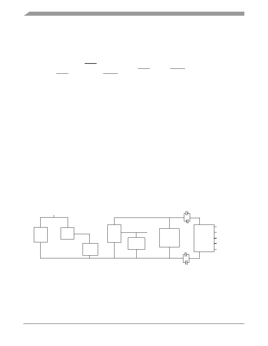
Figure 12-1 illustrates the general power control incorporated in the 56F8323/56F8123. This chip
contains two internal power regulators. One of them is powered from the VDDA_OSC_PLL pin and cannot
be turned off. This regulator controls power to the internal clock generation circuitry. The other regulator
is powered from the VDD_IO pins and provides power to all of the internal digital logic of the core, all
peripherals and the internal memories. This regulator can be turned off, if an external VDD_CORE voltage
is externally applied to the VCAP pins.
In summary, the entire chip can be supplied from a single 3.3 volt supply if the large core regulator is
enabled. If the regulator is not enabled, a dual supply 3.3V/2.5V configuration can also be used.
Notes:
Flash, RAM and internal logic are powered from the core regulator output
VPP1 and VPP2 are not connected in the customer system
All circuitry, analog and digital, shares a common VSS bus
Figure 12-1 Power Management
REG
CORE
VCAP
I/O
ADC
VDD
VSS
OCS
REG
VDDA_OSC_PLL
ROSC
VSSA_ADC
VDDA_ADC
VREFH
VREFP
VREFMID
VREFN
VREFLO
相關(guān)PDF資料 |
PDF描述 |
|---|---|
| MC56MS-14 | 3500 MHz - 12000 MHz RF/MICROWAVE DOUBLE BALANCED MIXER, 9.5 dB CONVERSION LOSS-MAX |
| MC56MS-5 | 3500 MHz - 12000 MHz RF/MICROWAVE DOUBLE BALANCED MIXER, 9.5 dB CONVERSION LOSS-MAX |
| MC68HC11FC0CFU4 | Technical Summary 8-Bit Microcontroller |
| MC68HC11FC0CFU5 | Technical Summary 8-Bit Microcontroller |
| MC68L11FC0PU3 | Technical Summary 8-Bit Microcontroller |
相關(guān)代理商/技術(shù)參數(shù) |
參數(shù)描述 |
|---|---|
| MC56F8323EVM | 功能描述:開發(fā)板和工具包 - 其他處理器 MC56F832X Dev Kit RoHS:否 制造商:Freescale Semiconductor 產(chǎn)品:Development Systems 工具用于評估:P3041 核心:e500mc 接口類型:I2C, SPI, USB 工作電源電壓: |
| MC56F8323EVM | 制造商:Freescale Semiconductor 功能描述:Tools Development kit Kit Con |
| MC56F8323EVME | 功能描述:開發(fā)板和工具包 - 其他處理器 MC56F8323 EVAL BRD RoHS:否 制造商:Freescale Semiconductor 產(chǎn)品:Development Systems 工具用于評估:P3041 核心:e500mc 接口類型:I2C, SPI, USB 工作電源電壓: |
| MC56F8323EVME | 制造商:Freescale Semiconductor 功能描述:Evaluation Kit for MC56F832x and MC56F81 |
| MC56F8323MFB60 | 功能描述:數(shù)字信號處理器和控制器 - DSP, DSC 60MHz 60MIPS RoHS:否 制造商:Microchip Technology 核心:dsPIC 數(shù)據(jù)總線寬度:16 bit 程序存儲器大小:16 KB 數(shù)據(jù) RAM 大小:2 KB 最大時鐘頻率:40 MHz 可編程輸入/輸出端數(shù)量:35 定時器數(shù)量:3 設(shè)備每秒兆指令數(shù):50 MIPs 工作電源電壓:3.3 V 最大工作溫度:+ 85 C 封裝 / 箱體:TQFP-44 安裝風(fēng)格:SMD/SMT |
發(fā)布緊急采購,3分鐘左右您將得到回復(fù)。