- 您現(xiàn)在的位置:買賣IC網(wǎng) > PDF目錄299472 > MC56F8323 (Motorola, Inc.) 16-bit Hybrid Controllers PDF資料下載
參數(shù)資料
| 型號: | MC56F8323 |
| 廠商: | Motorola, Inc. |
| 英文描述: | 16-bit Hybrid Controllers |
| 中文描述: | 16位混合控制器 |
| 文件頁數(shù): | 129/140頁 |
| 文件大?。?/td> | 1981K |
| 代理商: | MC56F8323 |
第1頁第2頁第3頁第4頁第5頁第6頁第7頁第8頁第9頁第10頁第11頁第12頁第13頁第14頁第15頁第16頁第17頁第18頁第19頁第20頁第21頁第22頁第23頁第24頁第25頁第26頁第27頁第28頁第29頁第30頁第31頁第32頁第33頁第34頁第35頁第36頁第37頁第38頁第39頁第40頁第41頁第42頁第43頁第44頁第45頁第46頁第47頁第48頁第49頁第50頁第51頁第52頁第53頁第54頁第55頁第56頁第57頁第58頁第59頁第60頁第61頁第62頁第63頁第64頁第65頁第66頁第67頁第68頁第69頁第70頁第71頁第72頁第73頁第74頁第75頁第76頁第77頁第78頁第79頁第80頁第81頁第82頁第83頁第84頁第85頁第86頁第87頁第88頁第89頁第90頁第91頁第92頁第93頁第94頁第95頁第96頁第97頁第98頁第99頁第100頁第101頁第102頁第103頁第104頁第105頁第106頁第107頁第108頁第109頁第110頁第111頁第112頁第113頁第114頁第115頁第116頁第117頁第118頁第119頁第120頁第121頁第122頁第123頁第124頁第125頁第126頁第127頁第128頁當(dāng)前第129頁第130頁第131頁第132頁第133頁第134頁第135頁第136頁第137頁第138頁第139頁第140頁
Register Descriptions
56F8323 Technical Data, Rev. 11.0
Freescale Semiconductor
89
Preliminary
6.5.6.3
IRQ—Bit 10
This bit controls the pull-up resistors on the IRQA pin.
6.5.6.4
Reserved—Bits 9–4
This bit field is reserved or not implemented. It is read as 0 and cannot be modified by writing.
6.5.6.5
JTAG—Bit 3
This bit controls the pull-up resistors on the TRST, TMS, and TDI pins.
6.5.6.6
Reserved—Bits 2–0
This bit field is reserved or not implemented. It is read as 0 and cannot be modified by writing.
6.5.7
CLKO Select Register (SIM_CLKOSR)
The CLKO select register can be used to multiplex out any one of the clocks generated inside the clock
generation and SIM modules. The default value is SYS_CLK. All other clocks primarily muxed out are
for test purposes only, and are subject to significant unspecified latencies at high frequencies.
The upper four bits of the GPIOB register can function as GPIO, Quad Decoder #0 signals, or as additional
clock output signals. GPIO has priority and is enabled/disabled via the GPIOB_PER. If GPIOB[7:4] are
programmed to operate as peripheral outputs, then the choice between Quad Decoder #0 and additional
clock outputs is made here in the CLKOSR. The default state is for the peripheral function of GPIOB[7:4]
to be programmed as Quad Decoder #0. This can be changed by altering PHASE0 through INDEX shown
in Figure 6-9.
The CLKOUT pin is not bonded out in the device. Instead, it is offered only as a pad for die-level testing.
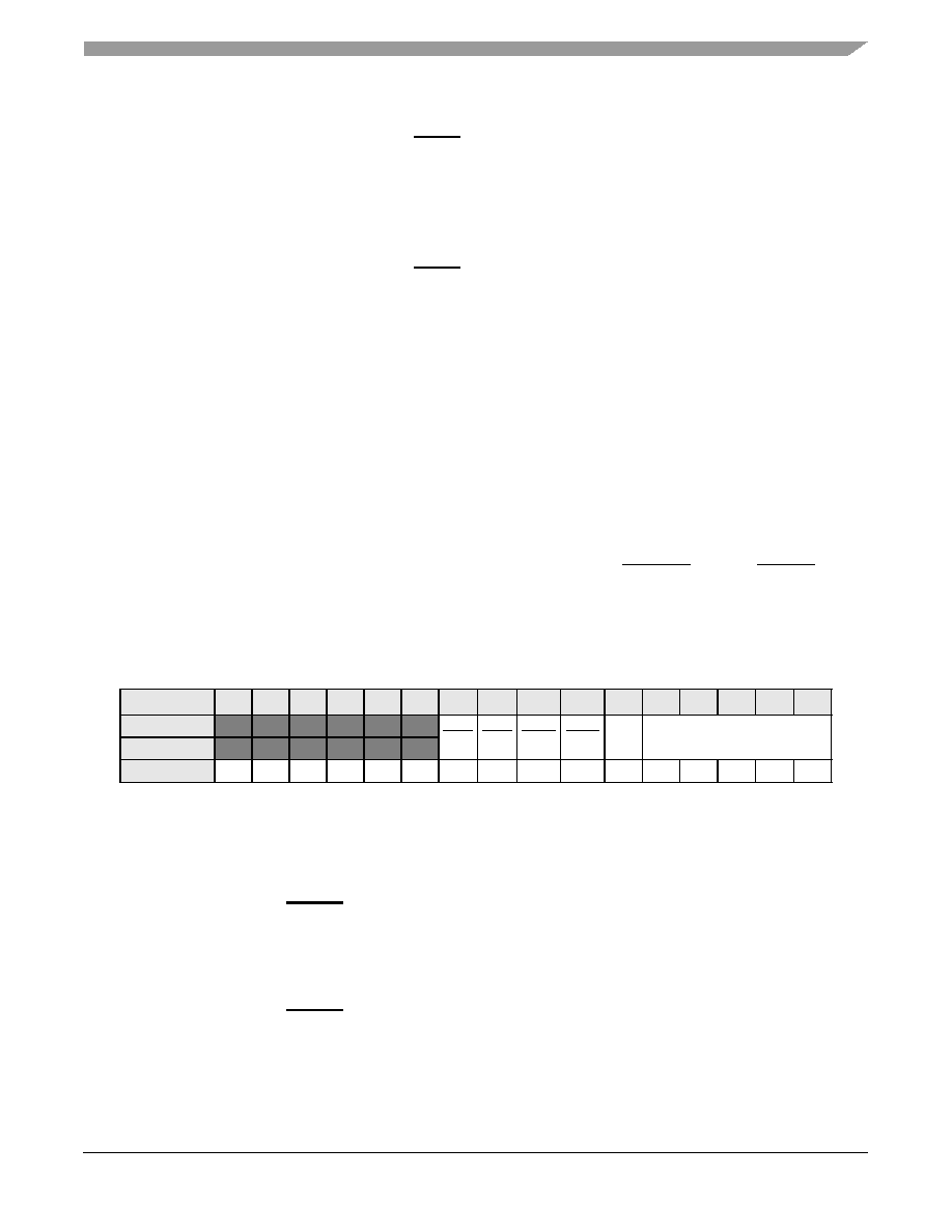
Figure 6-9 CLKO Select Register (SIM_CLKOSR)
6.5.7.1
Reserved—Bits 15–10
This bit field is reserved or not implemented. It is read as 0 and cannot be modified by writing.
6.5.7.2
PHASEA0 (PHSA)—Bit 9
0 = Peripheral output function of GPIOB[7] is defined to be PHASEA0
1 = Peripheral output function of GPIOB[7] is defined to be the oscillator clock (MSTR_OSC, see
6.5.7.3
PHASEB0 (PHSB)—Bit 8
0 = Peripheral output function of GPIOB[6] is defined to be PHASEB0
1 = Peripheral output function of GPIOB[6] is defined to be SYS_CLK2
Base + $A
15
14
13
12
11
10
9
8
7
6
5
4
3
2
1
0
Read
0
PHSA PHSB
INDEX
HOME
CLK
DIS
CLKOSEL
Write
RESET
000000
0
1
0
相關(guān)PDF資料 |
PDF描述 |
|---|---|
| MC56MS-14 | 3500 MHz - 12000 MHz RF/MICROWAVE DOUBLE BALANCED MIXER, 9.5 dB CONVERSION LOSS-MAX |
| MC56MS-5 | 3500 MHz - 12000 MHz RF/MICROWAVE DOUBLE BALANCED MIXER, 9.5 dB CONVERSION LOSS-MAX |
| MC68HC11FC0CFU4 | Technical Summary 8-Bit Microcontroller |
| MC68HC11FC0CFU5 | Technical Summary 8-Bit Microcontroller |
| MC68L11FC0PU3 | Technical Summary 8-Bit Microcontroller |
相關(guān)代理商/技術(shù)參數(shù) |
參數(shù)描述 |
|---|---|
| MC56F8323EVM | 功能描述:開發(fā)板和工具包 - 其他處理器 MC56F832X Dev Kit RoHS:否 制造商:Freescale Semiconductor 產(chǎn)品:Development Systems 工具用于評估:P3041 核心:e500mc 接口類型:I2C, SPI, USB 工作電源電壓: |
| MC56F8323EVM | 制造商:Freescale Semiconductor 功能描述:Tools Development kit Kit Con |
| MC56F8323EVME | 功能描述:開發(fā)板和工具包 - 其他處理器 MC56F8323 EVAL BRD RoHS:否 制造商:Freescale Semiconductor 產(chǎn)品:Development Systems 工具用于評估:P3041 核心:e500mc 接口類型:I2C, SPI, USB 工作電源電壓: |
| MC56F8323EVME | 制造商:Freescale Semiconductor 功能描述:Evaluation Kit for MC56F832x and MC56F81 |
| MC56F8323MFB60 | 功能描述:數(shù)字信號處理器和控制器 - DSP, DSC 60MHz 60MIPS RoHS:否 制造商:Microchip Technology 核心:dsPIC 數(shù)據(jù)總線寬度:16 bit 程序存儲器大小:16 KB 數(shù)據(jù) RAM 大小:2 KB 最大時鐘頻率:40 MHz 可編程輸入/輸出端數(shù)量:35 定時器數(shù)量:3 設(shè)備每秒兆指令數(shù):50 MIPs 工作電源電壓:3.3 V 最大工作溫度:+ 85 C 封裝 / 箱體:TQFP-44 安裝風(fēng)格:SMD/SMT |
發(fā)布緊急采購,3分鐘左右您將得到回復(fù)。