- 您現(xiàn)在的位置:買賣IC網(wǎng) > PDF目錄17005 > MAX19527EVKIT+ (Maxim Integrated Products)EVAL KIT MAX19527 PDF資料下載
參數(shù)資料
| 型號: | MAX19527EVKIT+ |
| 廠商: | Maxim Integrated Products |
| 文件頁數(shù): | 19/30頁 |
| 文件大小: | 0K |
| 描述: | EVAL KIT MAX19527 |
| 標準包裝: | 1 |
| 系列: | * |
第1頁第2頁第3頁第4頁第5頁第6頁第7頁第8頁第9頁第10頁第11頁第12頁第13頁第14頁第15頁第16頁第17頁第18頁當前第19頁第20頁第21頁第22頁第23頁第24頁第25頁第26頁第27頁第28頁第29頁第30頁
Ultra-Low-Power, Octal, 12-Bit, 50Msps,
1.8V ADC with Serial LVDS Outputs
MAX19527
26
Reserved Registers (0Ah to 0Fh)
These registers are reserved and should not be used or
programmed. It is possible to read from or write to these
registers, but the commands have no effect on device
operation.
Special Function Register (10h)
The Special Function register has two key functions: soft-
ware device reset and device status. To initiate a soft-
ware device reset, write the command 5Ah to the Special
Function register. Do not write any other values to this
register as they could permanently alter the device con-
figuration. When read, the register returns a status byte
with the information described in Table 24.
Applications Information
Analog Inputs
The ADC provides better SFDR and THD with fully
differential input signals than a single-ended input drive.
In differential input mode, even-order harmonics are
lower as both inputs are balanced, and each of the ADC
inputs only require half the signal swing compared to
single-ended input mode. Single-ended operation for the
device is not recommended.
AC-Coupled Inputs
An RF transformer provides an excellent solution for
converting a single-ended signal to a fully differential
signal (Figure 11). CMOUT provides the common-mode
voltage for an AC-coupled input. The transformer shown
has an impedance ratio of 1:1. Alternatively, a different
step-up transformer can be selected to reduce the drive
requirements. A reduced signal swing from the input
driver can also improve the overall distortion.
Clock Inputs
Differential, AC-Coupled Clock Inputs
For optimum dynamic performance, the clock inputs
to the device should be driven with an AC-coupled
differential signal. However, frequently the available
clock source is single-ended. Figure 12 demonstrates
one method for converting a single-ended clock sig-
nal into a differential signal with a transformer. In this
example, a Coilcraft transformer (TTWB-2-B), whose
impedance ratio from primary to secondary is 1:2.
The signal in this example is terminated into a series
combination of two 50
Ω resistors with their common node
AC-coupled to ground. Figure 12 illustrates the second-
ary side of the transformer to be coupled directly to the
clock inputs. Since the clock inputs are self-biasing,
the center tap of the transformer must be AC-coupled
to ground or left unconnected. If the center tap of the
transformer’s secondary side is DC-coupled to ground,
it is necessary to add blocking capacitors in series with
the clock inputs.
Clock jitter performance can be enhanced if the clock
signal has a high slew rate at the time of its zero-
crossing. Therefore, if a sinusoidal source is used to
drive the clock inputs, the clock amplitude should be
as large as possible to maximize the zero-crossing slew
rate. The back-to-back Schottky diodes shown in Figure
12 are not required as long as the input signal is held
to a differential voltage potential of 3VP-P or less. If a
larger amplitude signal is provided (to maximize the
zero-crossing slew rate), then the diodes serve to limit
the differential signal swing at the clock inputs.
Any differential mode noise coupled to the clock inputs
translates to clock jitter and degrades the SNR perfor-
mance of the device. Any differential mode coupling of
the analog input signal into the clock inputs results in
harmonic distortion. Consequently, it is important that the
clock lines be well isolated from the analog signal input
and from the digital outputs.
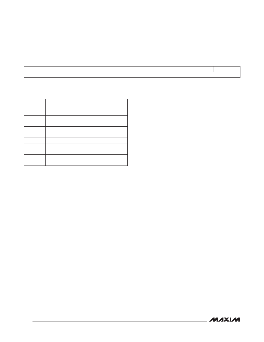
Table 23. Custom Test Pattern 3 (09h)
Table 24. Special Function Register (10h)
Status Byte (Read)
STATUS
BIT NO.
READ
VALUE
DESCRIPTION
7
0
Reserved
6
0
Reserved
5
0 or 1
1 = ROM read in progress
4
0 or 1
1 = ROM read completed, and
register data is valid (checksum ok)
3
0
Reserved
2
1
Reserved
1
0 or 1
Reserved
0
0 or 1
1 = Duty-cycle equalizer DLL is
locked
BIT 7
BIT 6
BIT 5
BIT 4
BIT 3
BIT 2
BIT 1
BIT 0
BITS_CUSTOM2[11:8]
BITS_CUSTOM1[11:8]
相關(guān)PDF資料 |
PDF描述 |
|---|---|
| SRR0805-681K | INDUCTOR PWR 680UH 10% SHLD SMD |
| ADR431BRZ-REEL7 | IC VREF SERIES PREC 2.5V 8-SOIC |
| VI-JWH-EY | CONVERTER MOD DC/DC 52V 50W |
| MAX11131EVKIT# | EVAL KIT MAX11131 |
| MAX11635EVSYS# | KIT EVAL SYSTEM |
相關(guān)代理商/技術(shù)參數(shù) |
參數(shù)描述 |
|---|---|
| MAX19527EVKIT+ | 功能描述:數(shù)據(jù)轉(zhuǎn)換 IC 開發(fā)工具 MAX19527 Eval Kit RoHS:否 制造商:Texas Instruments 產(chǎn)品:Demonstration Kits 類型:ADC 工具用于評估:ADS130E08 接口類型:SPI 工作電源電壓:- 6 V to + 6 V |
| MAX19527EXE+ | 功能描述:模數(shù)轉(zhuǎn)換器 - ADC 12Bit 8Ch 50Msps 1.8V ADC RoHS:否 制造商:Texas Instruments 通道數(shù)量:2 結(jié)構(gòu):Sigma-Delta 轉(zhuǎn)換速率:125 SPs to 8 KSPs 分辨率:24 bit 輸入類型:Differential 信噪比:107 dB 接口類型:SPI 工作電源電壓:1.7 V to 3.6 V, 2.7 V to 5.25 V 最大工作溫度:+ 85 C 安裝風格:SMD/SMT 封裝 / 箱體:VQFN-32 |
| MAX19527EXE+T | 功能描述:模數(shù)轉(zhuǎn)換器 - ADC 12Bit 8Ch 50Msps 1.8V ADC RoHS:否 制造商:Texas Instruments 通道數(shù)量:2 結(jié)構(gòu):Sigma-Delta 轉(zhuǎn)換速率:125 SPs to 8 KSPs 分辨率:24 bit 輸入類型:Differential 信噪比:107 dB 接口類型:SPI 工作電源電壓:1.7 V to 3.6 V, 2.7 V to 5.25 V 最大工作溫度:+ 85 C 安裝風格:SMD/SMT 封裝 / 箱體:VQFN-32 |
| MAX19528EVKIT+ | 制造商:Maxim Integrated Products 功能描述:ANALOG TO DIGITAL CONVERTER - Boxed Product (Development Kits) |
| MAX19528EXE+ | 功能描述:模數(shù)轉(zhuǎn)換器 - ADC Integrated Circuits (ICs) Analog to Digital Converters - IC ADC 12BIT 8CH 64MSPS 144CTBGA RoHS:否 制造商:Texas Instruments 通道數(shù)量:2 結(jié)構(gòu):Sigma-Delta 轉(zhuǎn)換速率:125 SPs to 8 KSPs 分辨率:24 bit 輸入類型:Differential 信噪比:107 dB 接口類型:SPI 工作電源電壓:1.7 V to 3.6 V, 2.7 V to 5.25 V 最大工作溫度:+ 85 C 安裝風格:SMD/SMT 封裝 / 箱體:VQFN-32 |
發(fā)布緊急采購,3分鐘左右您將得到回復。