- 您現(xiàn)在的位置:買(mǎi)賣(mài)IC網(wǎng) > PDF目錄358865 > LM4560 (National Semiconductor Corporation) Advanced PCI Audio Accelerator PDF資料下載
參數(shù)資料
| 型號(hào): | LM4560 |
| 廠商: | National Semiconductor Corporation |
| 英文描述: | Advanced PCI Audio Accelerator |
| 中文描述: | 先進(jìn)的PCI音頻加速器 |
| 文件頁(yè)數(shù): | 6/54頁(yè) |
| 文件大小: | 380K |
| 代理商: | LM4560 |
第1頁(yè)第2頁(yè)第3頁(yè)第4頁(yè)第5頁(yè)當(dāng)前第6頁(yè)第7頁(yè)第8頁(yè)第9頁(yè)第10頁(yè)第11頁(yè)第12頁(yè)第13頁(yè)第14頁(yè)第15頁(yè)第16頁(yè)第17頁(yè)第18頁(yè)第19頁(yè)第20頁(yè)第21頁(yè)第22頁(yè)第23頁(yè)第24頁(yè)第25頁(yè)第26頁(yè)第27頁(yè)第28頁(yè)第29頁(yè)第30頁(yè)第31頁(yè)第32頁(yè)第33頁(yè)第34頁(yè)第35頁(yè)第36頁(yè)第37頁(yè)第38頁(yè)第39頁(yè)第40頁(yè)第41頁(yè)第42頁(yè)第43頁(yè)第44頁(yè)第45頁(yè)第46頁(yè)第47頁(yè)第48頁(yè)第49頁(yè)第50頁(yè)第51頁(yè)第52頁(yè)第53頁(yè)第54頁(yè)
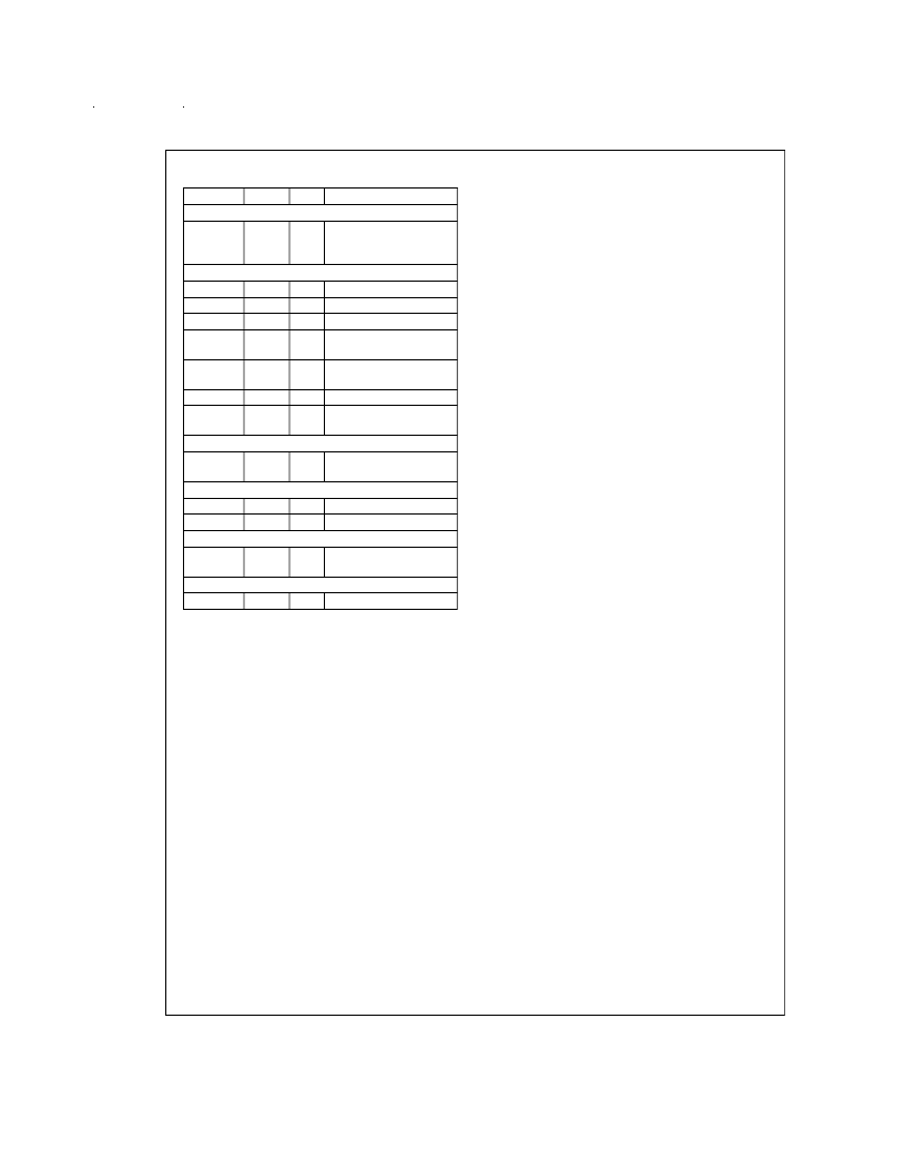
1.0 Pin Description
(Continued)
Symbol
AC97 CODEC INTERFACE SIGNALS (6)
ACDO
54
Pin(s)
Type
Description
OUT
AC97 serial data out.
This output sends serial
data to codec(s).
I2S INTERFACE (7)
I2SBCKI
I2SLRCKI
I2SDI
I2SBCKO
82
81
80
79
IN
IN
IN
I2S Receiver Bit Clock
I2S Receiver L/R Clock
I2S Receiver Data
I2S Transmitter Bit
Clock
I2S Transmitter L/R
Clock
I2S Transmitter Data
I2S Transmitter Master
Clock
OUT
I2SLRCKO
78
OUT
I2SDO
MCLK
77
76
OUT
OUT
S/PDIF TRANSMITTER (1)
SPDO
51
OUT
S/PDIF transmitter
output
GAME PORT PINS (8)
GD[7:4]
GD[3:0]
GENERAL-PURPOSE I/O (8)
GPIO[7:0]
68:61
47:44
43:40
IN
IN
Gameport data
Gameport data
I/O
General-purpose
input/output
NO CONNECTIONS (5)
NC
70:74
No connections
2.0 Functional Description
2.1 DEVICE OVERVIEW
2.1.1
The LM4560 is composed of several functional blocks.
There is a PCI bus interface, a wave engine, I/O interfaces
and legacy support hardware.
2.1.1.1
The PCI bus interface includes all the logic that talks
to the PCI bus, handles the PCI bus cycles, reports PCI con-
figuration block and PCI power management. The EEPROM
interface for supporting the SubSystem and SubVendor ID
fields for PCI card vendors is located here.
2.1.1.2
The wave engine supports all the logic necessary to
synthesize wave table voices / instruments. The sample rate
converter is used to pitch shift the samples and rate convert
pcm streams. For example converting from 44.1 ksps CD
audio to 48ksps DAT pcm. The wave engine is also used to
play back WDM streams and for the legacy PC audio func-
tions. There are three mixers in the wave engine, the main
mixer, and mixers for chorus and reverb sends.
2.1.1.3
The I/O ports include the AC97 Rev 2.0 I/O, the I2S
I/O, the SPDIF out, GPIOs, gameport and MPU401 midi I/O.
2.1.1.3.1
The AC97 port supports two AC97 codecs. The pri-
mary codec must be Rev 1.03, 2.0 or 2.1. The secondary co-
dec must be Rev 2.0 or 2.1.
2.1.1.3.2
The I2S port supports data out at 48 KSPS only
and inputs at rates from 8 to 48 KSPS. Output can come
from I2S L/R Output Buffer or SURR L/R Output FIFO. The
input data rate can be determined by reading the 13 lsbs of
register 0xCC. The sample rate = (I2S_DELTA)*60. The
transmitter sends 20 bits stereo and the receiver receives 20
stereo. When the I2S data in receives more than 20 bits, the
lsb’s are truncated. If the receiver receives less than 20 bits,
zeros are appended to the lsbs.
2.1.1.3.3
The SPDIF output only supports Mode 0 consumer
20 bit audio data that is sampled at 48 kHz. If the receiver
needs fewer bits, then the lsbs will be truncated.
2.1.1.3.4
The GPIO pins are 5V tolerant programmable I/O
pins. They can be programmed to either inputs or output via
a register at offset 7Ch. On power up all the pins default to
inputs.
If any of the GPIO pins are used for hardware control pins,
the best programming procedure would be to leave the i/o
pins as inputs, then set the output bits to highs or lows, then
change the selected I/O pins to outputs. This will avoid the
possibility of glitches on the output. Since the pins power up
as inputs, they will be floating and so 30 k
resistors are
needed to put the pin into a know state on power up.
The inputs can be read from the same register 7Ch. The
CPU must poll the 7Ch to see if any of the inputs have
changed state.
2.1.1.3.5
The Game port pins are 5V tolerant I/O pins and
support the standard dual analog joysticks.
The enhanced mode works will all normal analog input joy-
sticks. The CPU can read internal counters rather than mea-
suring the time constants of each of the X, Y inputs with soft-
ware timing loops.
2.1.1.3.6
The LM4560 supports the standard MPU 401 uart
mode midi interface.
www.national.com
6
相關(guān)PDF資料 |
PDF描述 |
|---|---|
| LM45BIM3 | SOT-23 Precision Centigrade Temperature Sensors |
| LM45BIM3X | SOT-23 Precision Centigrade Temperature Sensors |
| LM45B | SOT-23 Precision Centigrade Temperature Sensors |
| LM4610 | Dual DC Operated Tone/Volume/Balance Circuit with National 3-D Sound |
| LM4610N | Dual DC Operated Tone/Volume/Balance Circuit with National 3-D Sound |
相關(guān)代理商/技術(shù)參數(shù) |
參數(shù)描述 |
|---|---|
| LM4560VJD | 制造商:Rochester Electronics LLC 功能描述:- Bulk |
| LM4562 | 制造商:NSC 制造商全稱:National Semiconductor 功能描述:Dual High Performance, High Fidelity Audio Operational Amplifier |
| LM4562_07 | 制造商:NSC 制造商全稱:National Semiconductor 功能描述:Dual High Performance, High Fidelity Audio Operational Amplifier |
| LM4562HA | 制造商:Texas Instruments 功能描述:OP Amp Dual GP ??17V 8-Pin TO-99 Tray |
| LM4562HA/NOPB | 功能描述:運(yùn)算放大器 - 運(yùn)放 RoHS:否 制造商:STMicroelectronics 通道數(shù)量:4 共模抑制比(最小值):63 dB 輸入補(bǔ)償電壓:1 mV 輸入偏流(最大值):10 pA 工作電源電壓:2.7 V to 5.5 V 安裝風(fēng)格:SMD/SMT 封裝 / 箱體:QFN-16 轉(zhuǎn)換速度:0.89 V/us 關(guān)閉:No 輸出電流:55 mA 最大工作溫度:+ 125 C 封裝:Reel |
發(fā)布緊急采購(gòu),3分鐘左右您將得到回復(fù)。