- 您現(xiàn)在的位置:買賣IC網(wǎng) > PDF目錄299403 > LFXP20E-3FN484C (LATTICE SEMICONDUCTOR CORP) PDF資料下載
參數(shù)資料
| 型號: | LFXP20E-3FN484C |
| 廠商: | LATTICE SEMICONDUCTOR CORP |
| 元件分類: | FPGA |
| 中文描述: | FPGA, 2464 CLBS, PBGA484 |
| 封裝: | 23 X 23 MM, LEAD FREE, FPBGA-484 |
| 文件頁數(shù): | 109/130頁 |
| 文件大?。?/td> | 1312K |
| 代理商: | LFXP20E-3FN484C |
第1頁第2頁第3頁第4頁第5頁第6頁第7頁第8頁第9頁第10頁第11頁第12頁第13頁第14頁第15頁第16頁第17頁第18頁第19頁第20頁第21頁第22頁第23頁第24頁第25頁第26頁第27頁第28頁第29頁第30頁第31頁第32頁第33頁第34頁第35頁第36頁第37頁第38頁第39頁第40頁第41頁第42頁第43頁第44頁第45頁第46頁第47頁第48頁第49頁第50頁第51頁第52頁第53頁第54頁第55頁第56頁第57頁第58頁第59頁第60頁第61頁第62頁第63頁第64頁第65頁第66頁第67頁第68頁第69頁第70頁第71頁第72頁第73頁第74頁第75頁第76頁第77頁第78頁第79頁第80頁第81頁第82頁第83頁第84頁第85頁第86頁第87頁第88頁第89頁第90頁第91頁第92頁第93頁第94頁第95頁第96頁第97頁第98頁第99頁第100頁第101頁第102頁第103頁第104頁第105頁第106頁第107頁第108頁當前第109頁第110頁第111頁第112頁第113頁第114頁第115頁第116頁第117頁第118頁第119頁第120頁第121頁第122頁第123頁第124頁第125頁第126頁第127頁第128頁第129頁第130頁
2-5
Architecture
Lattice Semiconductor
LatticeXP Family Data Sheet
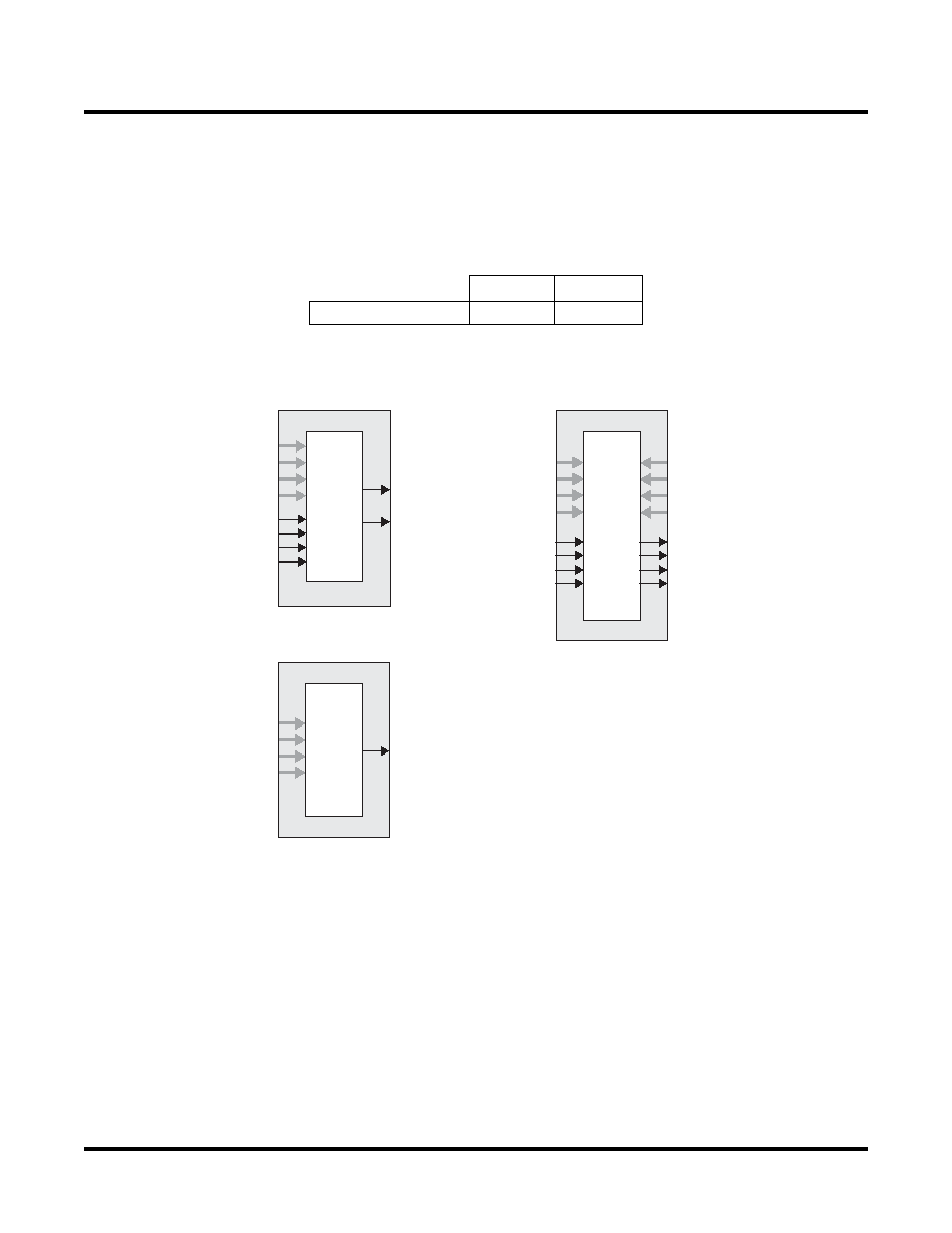
The Lattice design tools support the creation of a variety of different size memories. Where appropriate, the soft-
ware will construct these using distributed memory primitives that represent the capabilities of the PFU. Table 2-3
shows the number of Slices required to implement different distributed RAM primitives. Figure 2-4 shows the dis-
tributed memory primitive block diagrams. Dual port memories involve the pairing of two Slices, one Slice functions
as the read-write port. The other companion Slice supports the read-only port. For more information on RAM mode
in LatticeXP devices, please see details of additional technical documentation at the end of this data sheet.
Table 2-3. Number of Slices Required for Implementing Distributed RAM
Figure 2-4. Distributed Memory Primitives
ROM Mode: The ROM mode uses the same principal as the RAM modes, but without the Write port. Pre-loading is
accomplished through the programming interface during configuration.
PFU Modes of Operation
Slices can be combined within a PFU to form larger functions. Table 2-4 tabulates these modes and documents the
functionality possible at the PFU level.
SPR16x2
DPR16x2
Number of Slices
1
2
Note: SPR = Single Port RAM, DPR = Dual Port RAM
DO1
DO0
DI0
DI1
AD0
AD1
AD2
AD3
WRE
CK
DO0
AD0
AD1
AD2
AD3
DPR16x2
SPR16x2
ROM16x1
RDO1
RDO0
DI0
DI1
WCK
WRE
WDO1
WDO0
WAD0
WAD1
WAD2
WAD3
RAD0
RAD1
RAD2
RAD3
相關PDF資料 |
PDF描述 |
|---|---|
| LFXP20E-5FN484C | |
| LFXP15C-4FN256C | |
| LFZ3508VXX | GENERAL PURPOSE INDUCTOR |
| LFZ2805HXX | GENERAL PURPOSE INDUCTOR |
| LF02004VTX | GENERAL PURPOSE INDUCTOR |
相關代理商/技術參數(shù) |
參數(shù)描述 |
|---|---|
| LFXP20E-3FN484I | 功能描述:FPGA - 現(xiàn)場可編程門陣列 19.7K LUTs 340 IO 1. 2V -3 Spd I RoHS:否 制造商:Altera Corporation 系列:Cyclone V E 柵極數(shù)量: 邏輯塊數(shù)量:943 內(nèi)嵌式塊RAM - EBR:1956 kbit 輸入/輸出端數(shù)量:128 最大工作頻率:800 MHz 工作電源電壓:1.1 V 最大工作溫度:+ 70 C 安裝風格:SMD/SMT 封裝 / 箱體:FBGA-256 |
| LFXP20E-4F256C | 功能描述:FPGA - 現(xiàn)場可編程門陣列 19.7K LUTs 188 IO 1. 2V -4 Spd RoHS:否 制造商:Altera Corporation 系列:Cyclone V E 柵極數(shù)量: 邏輯塊數(shù)量:943 內(nèi)嵌式塊RAM - EBR:1956 kbit 輸入/輸出端數(shù)量:128 最大工作頻率:800 MHz 工作電源電壓:1.1 V 最大工作溫度:+ 70 C 安裝風格:SMD/SMT 封裝 / 箱體:FBGA-256 |
| LFXP20E-4F256I | 功能描述:FPGA - 現(xiàn)場可編程門陣列 19.7K LUTs 188 IO 1. 2V -4 Spd I RoHS:否 制造商:Altera Corporation 系列:Cyclone V E 柵極數(shù)量: 邏輯塊數(shù)量:943 內(nèi)嵌式塊RAM - EBR:1956 kbit 輸入/輸出端數(shù)量:128 最大工作頻率:800 MHz 工作電源電壓:1.1 V 最大工作溫度:+ 70 C 安裝風格:SMD/SMT 封裝 / 箱體:FBGA-256 |
| LFXP20E-4F388C | 功能描述:FPGA - 現(xiàn)場可編程門陣列 19.7K LUTs 268 IO 1. 2V -4 Spd RoHS:否 制造商:Altera Corporation 系列:Cyclone V E 柵極數(shù)量: 邏輯塊數(shù)量:943 內(nèi)嵌式塊RAM - EBR:1956 kbit 輸入/輸出端數(shù)量:128 最大工作頻率:800 MHz 工作電源電壓:1.1 V 最大工作溫度:+ 70 C 安裝風格:SMD/SMT 封裝 / 箱體:FBGA-256 |
| LFXP20E-4F388I | 功能描述:FPGA - 現(xiàn)場可編程門陣列 19.7K LUTs 268 IO 1. 2V -4 Spd I RoHS:否 制造商:Altera Corporation 系列:Cyclone V E 柵極數(shù)量: 邏輯塊數(shù)量:943 內(nèi)嵌式塊RAM - EBR:1956 kbit 輸入/輸出端數(shù)量:128 最大工作頻率:800 MHz 工作電源電壓:1.1 V 最大工作溫度:+ 70 C 安裝風格:SMD/SMT 封裝 / 箱體:FBGA-256 |
發(fā)布緊急采購,3分鐘左右您將得到回復。